
Many people find it amazing when they first get a gallium nitride (GaN) charger: with the same 65W output, why can it be half the size or even smaller than a traditional laptop adapter? Is it a gimmick made by “concentrating electricity”? Actually, the answer is simple: chargers themselves do not store a large amount of electricity. The core function of gallium nitride is to achieve higher-frequency and lower-loss power conversion, driving the miniaturization of core internal components such as transformers and heat dissipation structures together; of course, the final size is also directly related to the manufacturer’s circuit design, heat dissipation strategy, safety standards, and even cost trade-offs.
First, Understand: The Correct Comparison Premise for “Smaller”
Before discussing the advantages of gallium nitride, we must first clarify the basic concepts and comparison rules, otherwise it is easy to be led astray by marketing propaganda and randomly compare the sizes of completely different products.
What Exactly Is a Gallium Nitride Charger
Let’s start with the most basic clarification: a gallium nitride charger is essentially a power adapter — a device that converts high-voltage alternating current from the wall into low-voltage direct current that can be used by mobile phones, tablets, and laptops. Its core functions are voltage conversion, current control, fast charging protocol negotiation, and safety protections such as over-temperature, over-current, and over-voltage protection.
Many people mistakenly think it is a “high-tech battery”, which is a complete misunderstanding: chargers do not store electricity, they are only responsible for “conversion” and “transmission”. And “gallium nitride (GaN)” is a semiconductor material, mainly used to replace silicon power switching devices in traditional chargers — note that it only replaces some core power components, not everything in the charger is replaced with gallium nitride.
“Smaller” Requires a Unified Comparison Caliber
The claim that “gallium nitride is smaller” has prerequisites. Comparing a 65W three-port GaN charger with a 20W single-port ordinary silicon charger, or comparing a US-spec foldable plug product with a UK-spec fixed plug product, is meaningless. A correct comparison must unify four dimensions:
| Comparison Dimension | Unified Standard | Common Misconception |
|---|---|---|
| Maximum Output Power | Compare at the same power (e.g., 65W vs. 65W) | Comparing the size of a high-power GaN charger with a low-power ordinary charger |
| Number of Ports | Compare with the same number of ports (e.g., single USB-C vs. single USB-C) | Comparing a multi-port GaN charger with a single-port ordinary charger |
| Plug Specification | Compare with plugs for the same region (e.g., US-spec vs. US-spec) | Comparing a US-spec product with flat prongs to a UK-spec product with square prongs |
| Volume Calculation | Uniformly include plugs, protrusions, and adapters | Only look at the front area, ignoring thickness and protruding plugs |
Also pay attention to the manufacturer’s nominal caliber: some products do not count foldable plugs when marking dimensions, some do not count detachable adapters. When comparing, try to calculate the three-dimensional volume (length × width × height) yourself, and do not only rely on vague descriptions like “palm-sized”.
Why People Care So Much About Charger Size
For people who commute or travel on business frequently, a smaller charger size brings tangible experience improvements:
- Saves more space for travel and business trips: A 65W GaN charger can charge a mobile phone and a laptop at the same time, which is much smaller than carrying two traditional adapters, leaving room for an extra book or a change of clothes in the backpack.
- Does not waste socket space: A small body plugged into a wall socket or power strip will not block adjacent sockets, especially for travel power strips with small socket spacing, the advantage is particularly obvious.
- Easier to carry around: Smaller size usually means lighter weight. When going to a coffee shop to work or going out for a short trip, it is not cumbersome to put in your pocket.
Entry-Level Boundary: Not All GaN Chargers Are Necessarily Smaller
Let’s give you a heads-up here to avoid pitfalls:
First, not all chargers printed with “gallium nitride” are small. If the manufacturer has a conservative design, a loose heat dissipation strategy, or only uses GaN as a marketing gimmick, the product size may be similar to that of an excellent traditional silicon charger.
Second, smaller size is not always better. The miniaturization of chargers must meet the requirements of safety distance, temperature rise, electromagnetic compatibility, electrical life, and structural strength. Blindly pursuing “mini” may sacrifice safety and durability.
Third, the advantage is not obvious in the low-power segment. For mobile phone chargers of around 20W, traditional silicon solutions can already be made very small, and the volume improvement brought by GaN is almost imperceptible, so there is no need to spend extra money just for the words “gallium nitride”.
Why Traditional Silicon Chargers Are Harder to Make Small
To understand the advantages of gallium nitride, we must first know what limits the size of traditional silicon chargers. Let’s start with the internal structure of the charger.
Which Components in a Charger Take Up the Most Space
When you take apart an ordinary medium-to-high power charger, you will find that the main components that take up space are these types:
- Transformer: Responsible for isolation and voltage conversion between high voltage and low voltage, it is one of the largest components in many chargers, especially for products above 65W.
- Inductors and Capacitors: Responsible for energy storage, filtering, and making the output current more stable. The higher the power and the lower the operating frequency, the larger these components usually are.
- Heat Dissipation Structure: Including metal heat sinks, thermal conductive glue, PCB copper foil, and even specially reserved air heat dissipation space, all of which are used to conduct the internal heat out.
- EMI and Safety Components: Such as fuses, varistors, common mode inductors, X capacitors, Y capacitors, etc., these are “essential parts” to meet safety and electromagnetic compatibility requirements, and will occupy a fixed space.
- Housing and Plug Structure: Foldable plugs require internal hinge space, UK three-pin plugs are themselves larger than US flat plugs, and replaceable plug modules also need to reserve interfaces, these mechanical structures will increase the volume.
A Plain-Language Explanation of How Switching Power Supplies Work
The core work of a charger is to “convert high-voltage AC into low-voltage DC”, and this process relies on switching power supply technology. You can think of it as an “energy handling system”:
The high-voltage AC from the wall is first converted into high-voltage DC, then through a “power switch” (equivalent to a high-speed gate) that keeps opening and closing, energy is sent to the transformer in small packets. The transformer steps down the voltage, and then it is filtered into stable low-voltage DC for the device to use.
There is a key rule here: The higher the switching frequency, the less energy needs to be handled each time, and the transformers and inductors responsible for storing and converting energy have the opportunity to be made smaller — just like when transporting goods, if you can make 30 trips a day, you only need to pull a small amount of goods per trip, and you don’t need a big truck.
So why don’t traditional chargers raise the frequency very high? Because the higher the frequency, the greater the loss of the power switch, and the more serious the heat generation, just like a person running too fast will get exhausted and sweat more. When the frequency is high enough, the electricity wasted by switching will be too much to be worth the loss, and it will also bring problems such as electromagnetic interference and layout difficulties, so it cannot be increased indefinitely.
The Real Bottleneck of Silicon Solutions: It’s Not That They Can’t Do High Frequency, But That High Frequency Costs More
Many people think that traditional silicon chargers cannot do high frequency, but that’s not true. Mature silicon power switches (silicon MOSFETs) can also achieve operating frequencies of tens of kHz or even hundreds of kHz, but the problem is: the higher the frequency, the switching loss, drive loss, and reverse recovery loss of silicon devices will all increase significantly, and heat generation will become very serious.
To control temperature rise, silicon solutions require larger heat sinks, more conservative magnetic component designs, and looser circuit board layouts. The result is: when the frequency is increased, the volume of heat dissipation and other components increases again, the overall volume does not decrease much, and the cost is much higher.
So the conclusion is clear: traditional silicon chargers are not absolutely unable to be made small, but in the medium-to-high power segment, it is very difficult to balance small size, high efficiency, low temperature rise, and low cost at the same time.
Why Losses Increase Volume
You may ask: It’s just a little heat, why does it affect the volume?
Because in the process of power conversion, all “wasted electricity” (that is, loss) will eventually turn into heat. The more heat there is, the larger the heat sink, the more thermal conductive material, the thicker the copper foil, and even more air space must be left in the housing for heat dissipation.
Moreover, high temperature will directly shorten the life of components: electrolytic capacitors, plastic housings, solder joints, and semiconductor devices will all accelerate aging due to long-term high temperature. In order to pass safety tests and life tests, traditional silicon chargers usually cannot fill the internal space too tightly, and must leave enough heat dissipation margin.
Safety Distance Is a Hard Bottom Line That Cannot Be Touched
There is another limitation that many people don’t know: the charger has a “high-voltage side” (the end connected to the wall socket, with a voltage of 100~240V) and a “low-voltage side” (the end connected to the device, usually only 5~20V). Strict creepage distance, electrical clearance, and insulation requirements must be met between the two — in simple terms, sufficient safety distance or insulating material must be reserved to prevent high-voltage electricity from leaking to the low-voltage side and hurting people.
These distances are determined by the input voltage, insulation level, use environment, and local certification standards, and cannot be arbitrarily reduced whether using silicon or gallium nitride. Gallium nitride can make the power device itself smaller and the layout more efficient, but it absolutely cannot eliminate high-low voltage isolation and basic safety space.
Core Logic: Why GaN Helps Chargers Become Smaller
After talking about the bottlenecks of traditional silicon solutions, the advantages of gallium nitride are very clear: it is not some “black magic”, but solves the core problem of “high loss at high frequencies” from the material characteristics, opening up space for charger miniaturization.
What Exactly Is Gallium Nitride (GaN)
Gallium nitride (GaN) is a wide-bandgap semiconductor material. You don’t need to remember this term, just know that it naturally has several characteristics suitable for making power switches: high voltage resistance, fast switching speed, and low loss at high frequencies. It is not a new invention either; it has long been widely used in LED lighting, radio frequency communication, base station power supplies and other fields. Only in recent years, as costs have come down, has it been used in consumer-grade chargers on a large scale.
In chargers, GaN is mainly used to replace traditional silicon high-voltage power switches, making the power conversion process run faster and more efficiently.
Advantage 1: Strong High-Frequency Operation Capability, Magnetic Components Have the Opportunity to Shrink
The most intuitive advantage of GaN devices is that their switching speed is particularly fast, and parasitic capacitance, gate charge (you can think of it as “extra burden when the switch is turned on and off”) are much lower than silicon devices, making them particularly suitable for high-frequency operation.
Nowadays, the common operating frequency of consumer-grade GaN chargers can reach hundreds of kHz, which is much higher than traditional silicon chargers. After the frequency is increased, transformers and inductors can complete conversion with smaller magnetic cores and less energy storage under the same power — just like the previous example of transporting goods, if the number of trips the trucks make increases, each truck doesn’t need to be that big, and the overall volume of the fleet will naturally be smaller.
But here’s a boundary to draw: The shrinkage ratio of the transformer is not proportional to the frequency, it’s not that if the frequency doubles, the volume is halved. Because after the frequency increases, the loss of the magnetic core itself, the heating of the copper wire, electromagnetic interference, and insulation requirements will all change, which will limit the further shrinkage of the volume. In actual products, there is an upper limit to the volume reduction brought by frequency increase.
Advantage 2: Lower Loss at High Frequencies, Heat Dissipation Space Can Be Reduced
The core advantage of GaN is not just “low on-resistance”, more importantly, the loss at the moment of switching is particularly low: for example, less gate charge, low output capacitance, almost no reverse recovery loss — in simple terms, very little electricity is wasted when the switch is turned on and off.
Under high-frequency operation, these characteristics can significantly reduce the overall loss, keeping the charger’s efficiency at a high level. Higher efficiency means less energy is turned into heat under the same output power, so naturally there is no need for such a large heat sink or so much thermal conductive material, and the housing and internal space can also be made more compact.
Of course, it should also be clarified: less heat does not mean no heat. When outputting at full load, in high-temperature summer environments, plugged into a closed wall socket, or when multiple ports are outputting at the same time, GaN chargers will still heat up significantly, just at a lower temperature than traditional silicon chargers of the same power.
Advantage 3: Smaller Devices, Lower Parasitic Parameters, Conducive to Compact Layout
Because GaN has a much higher breakdown electric field than silicon, for power devices with the same voltage withstand rating, GaN chips can be made smaller, and the packaging can also be more compact.
With smaller devices, the traces on the circuit board can be shorter, and the parasitic parameters of the switching node (you can think of it as “extra loss and noise caused by traces”) will also be lower, which in turn can further reduce losses, reduce electromagnetic interference, and make the layout more compact.
But again, it must be emphasized: the safety isolation distance between the high-voltage side and the low-voltage side must still be retained, and the safety distance cannot be arbitrarily reduced just because GaN has high voltage resistance — this is a safety bottom line, with no room for negotiation.
Advantage 4: More Suitable for Advanced Power Topologies
The “working circuit structure” of a charger (called “power topology” in the industry) also has a great impact on efficiency and volume. For example, more advanced topologies such as active clamp flyback (ACF), quasi-resonant flyback, and PFC+LLC are like more efficient cargo transport routes, which can further improve conversion efficiency and reduce losses.
GaN can more easily exert its advantages in these high-frequency, high-efficiency topologies, especially for medium-to-high power chargers such as 65W, 100W, and 140W, which can be made even smaller when paired with advanced topologies.
So finally, it must be clear: The small size of gallium nitride chargers is never as simple as “changing to GaN material”, but the result of system optimization of GaN devices + circuit topology + magnetic components + control chips + heat dissipation design + structural design. Without any of these links, a truly compact and reliable product cannot be made.
System-Level Shrinkage: Which Components GaN Drives to Become Smaller Together
GaN does not only make itself smaller, but through the advantages of “high frequency + low loss”, it drives multiple components in the entire charger to shrink together, ultimately achieving a reduction in overall volume.
Transformer and Inductor Shrinkage
This is the most intuitive change. After the operating frequency increases, the energy that needs to be transferred per switching cycle becomes less, the magnetic core of the transformer can be made smaller, the number of winding turns can also be reduced, and the overall volume can be shrunk a lot. At the same time, the ripple control of inductors is easier, and the volume of some filter inductors can also be reduced.
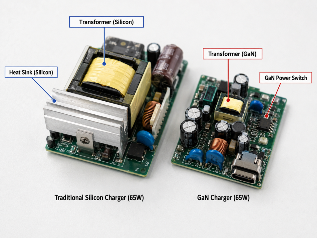
Of course, shrinkage is not unlimited: the high-frequency loss of the magnetic core itself, the heating of the copper wire, the insulation layer between windings, and the limitations of the production process will all restrict the further shrinkage of transformers and inductors.
Optimization of Capacitors and Filter Components
After the frequency increases, the frequency of the output voltage ripple (that is, the small fluctuation of the voltage) will also become higher, which is easier to filter out, so the volume of some output filter capacitors and inductors can be reduced.
But note: X capacitors and Y capacitors for safety, as well as large-capacity electrolytic capacitors at the input end, cannot be omitted arbitrarily. Especially for electrolytic capacitors, their volume is also affected by voltage withstand, life, ripple current, and operating temperature, and cannot be shrunk indefinitely.
More Compact Heat Dissipation Structure
Because the overall loss is reduced and heat generation is less, GaN chargers usually do not need to install large metal heat sinks like traditional silicon chargers. Many products use thermal conductive glue, PCB copper foil, or even directly rely on the housing for heat dissipation, which can save a lot of space.
But there are also risks here: if the manufacturer excessively pursues mini size and makes the heat dissipation path too narrow, it will lead to excessive housing temperature at full load, even trigger over-temperature protection, reduce output power, and long-term use will also shorten the life of internal components.
Increased Integration of Control Chips and Packaging
Today’s GaN chargers generally use highly integrated control chips, protocol chips, and synchronous rectification solutions to further save circuit board space. There is also a design called “co-packaged GaN”, which integrates GaN power devices, drive circuits, and even protection circuits in the same package, which not only saves PCB area, but also reduces parasitic parameters and improves efficiency.
Of course, there are also “discrete GaN” designs, where the power transistor and drive circuit are separated. This design is more flexible and has higher maturity, but the overall occupied circuit board area is a bit larger.
Here we also want to remind everyone: the “third-generation GaN” and “fifth-generation GaN” promoted by manufacturers currently have no unified industry standards, they are all each company’s own naming rules. You cannot judge the technical level solely by “generation”, you still have to look at the actual size, efficiency, and temperature rise performance.
Side Effects Brought by High Frequency Must Also Be Handled
High frequency is not only beneficial, the side effects are also obvious: the higher the frequency, the more likely it is to generate electromagnetic interference (EMI), which may interfere with nearby devices such as earphones and routers; too fast switching speed may also generate spike voltage, noise, and even inductor howling.
An excellent GaN charger achieves small size on the premise of solving these problems — relying on better PCB layout, shielding design, filter circuits, and grounding design, rather than omitting necessary components. If a GaN charger is particularly cheap and unbelievably small, it is likely that corners have been cut on EMI or safety standards, which poses safety hazards.
Real Volume Difference: Which Power Segments Have the Most Obvious Advantage
Gallium nitride’s volume advantage is not the same across all power segments, and the perceived gap varies greatly between different power segments.
20W and Below: The Difference Is Usually Not Obvious
For low-power chargers such as 20W mobile phone fast chargers, traditional silicon solutions can already be made very small, and the volume improvement brought by GaN is very limited, and may even be similar to silicon solutions due to conservative design.
For products in this power segment, everyone should pay more attention to price, safety certification, heat generation performance, and port specifications, and there is no need to spend extra money for the “gallium nitride” label.
45W to 100W: The Volume Advantage Is Most Easily Perceived
This is the power segment where gallium nitride has the most obvious advantages, and it is also the mainstream power range for mobile phones, tablets, thin and light laptops, and multi-port chargers.
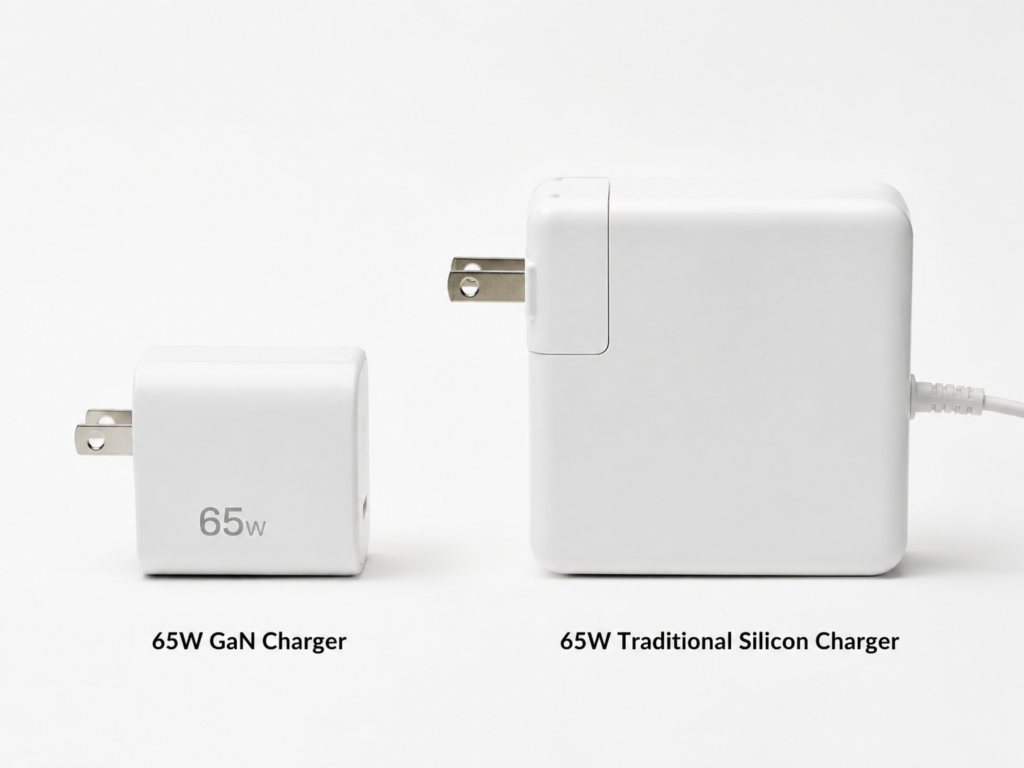
Under the premise of the same power, same ports, and same plug specifications, GaN products are usually 30%~50% smaller than traditional silicon solutions, with particularly obvious advantages in storage and socket occupation. The most typical example is the 65W charger: traditional silicon laptop adapters are usually long and thick, occupying two socket positions when plugged into a power strip; while a 65W GaN charger can be close to the size of an ordinary mobile phone charger, and will not block the adjacent hole when plugged into a wall socket.
Above 100W: GaN Advantages Are More Important, But Design Difficulty Is Also Higher
The higher the power, the more difficult it is for traditional silicon solutions to balance volume and temperature rise, and the more obvious the advantages of GaN. For example, 100W, 140W or even 200W multi-port chargers can achieve very high power density with GaN. One charger can fast charge a laptop, mobile phone, and tablet at the same time, so you don’t need to bring a bunch of adapters when going out.
But the design difficulty of high-power GaN chargers is also higher, requiring more complex PFC circuits, power distribution circuits, heat dissipation designs, and protection circuits. If a GaN charger above 100W is unbelievably small, you must pay special attention to its full-load temperature, long-term output stability, and whether it will automatically reduce power under high load.
Other Factors Affecting Volume Difference
In addition to power, there are many factors that affect the size of the charger. When comparing, these variables must be excluded:
- Number of ports: Multi-port chargers require more protocol control, power distribution, and output protection circuits, so a three-port charger is definitely larger than a single-port one.
- Plug structure: Foldable plugs require internal hinge space, UK three-pin plugs are themselves larger, and replaceable plug modules also need to reserve interfaces, all of which will increase the volume.
- Fast charging protocols: The more protocols supported (such as PD, PPS, QC, etc.), the more complex the control and protection circuits, and the volume may be slightly larger.
- Additional functions: Products with displays, wireless charging, stands, or even built-in cables will have a significantly increased volume, and cannot be directly compared with pure chargers.
- Safety and EMI design: Compliant products must retain necessary safety components and safety distances. If a product is unreasonably small, it is likely that corners have been cut on safety standards or electromagnetic compatibility, which poses safety hazards during use.
Advanced Judgment: How to Tell If the Volume Is Really Reasonable
If you want to further judge whether the miniaturization of a GaN charger is really “substantial”, you can start from these angles.
First Look at Power Parameters, Don’t Be Misled by Total Power
Many manufacturers mark the “total power” very high, but the actual single-port output or multi-port simultaneous output power is not that high. For example, for the same 65W dual-port charger, some have a maximum single-port output of 65W, and dual-port simultaneous output is 45W+20W; some have a maximum single-port output of 30W, and dual-port simultaneous output is 30W+30W — the actual experience is very different.
In addition, the charging speed also depends on whether your device supports the corresponding fast charging protocol and power level. If the device only supports 20W PD, even if the charger is 100W, it can only charge at 20W speed.
Use Power Density to Judge the Level of Miniaturization
If you want to compare the level of miniaturization more objectively, you can use the indicator of power density, the formula is very simple:
Power density = maximum output power ÷ body volume, common unit is W/cm³ (watts per cubic centimeter)
When calculating the volume, pay attention to unifying the caliber: should the length, width, and height include plugs, housing protrusions, and folding structures? Do detachable adapters count? Only comparisons under the same caliber are meaningful.
For example: a single USB-C 65W US-spec GaN charger, with foldable plugs folded in, has dimensions of 5cm×3cm×3cm, a volume of 45cm³, and a power density of 65÷45≈1.44W/cm³; while a traditional silicon charger of the same power may have a volume of 80cm³, with a power density of only about 0.8W/cm³, the gap is very obvious.
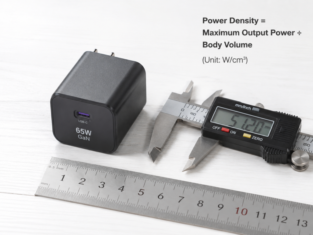
Of course, higher power density is not always better. It only reflects the level of miniaturization, and cannot represent the overall quality of the product — it must be considered together with temperature rise, stability, safety certification, and service life.
See If It Truly Leverages GaN Advantages
If a charger labeled GaN has a similar volume to a traditional silicon charger with the same configuration, there may be two situations: either the manufacturer’s design is too conservative and does not fully leverage the advantages of GaN; or it just uses GaN as a marketing gimmick, and actually has not done system optimization.
If you want to understand in depth, you can look at professional teardown reviews, paying attention to the GaN device model, circuit topology structure, transformer size, temperature rise test, and EMI design. These are much more reliable than promotional terms like “which generation of GaN” and “black technology chip”.
Balance Between Volume and Safety
Reasonable small size must be built on compliant safety distances, sufficient heat dissipation paths, and reliable protection circuits. If a product pursues “mini” so much that the interior is packed tightly, or even omits safety components, no matter how small it is, you should not buy it.
Here we also need to distinguish the meaning of certification marks in different regions:
- UL certification in the United States is a third-party safety certification, which requires passing strict safety tests and has high credibility;
- The CE mark in the European Union and the UKCA mark in the United Kingdom are compliance declarations, and manufacturers need to ensure that their products meet relevant standards on their own;
- FCC certification in the United States is mainly for electromagnetic compatibility, ensuring that products do not interfere with other electronic devices, and is not equivalent to safety certification.
When purchasing, prioritize products with locally recognized safety certifications for more assurance.
How to Verify in Real Use
If you have already bought it, you can verify whether its design is reasonable through several simple methods:
- Full load test: Charge a laptop or other device that supports high power for half an hour to an hour, touch the charger housing. If it is so hot that you can’t hold it at all, it means there is a problem with the heat dissipation design; if it is just warm or a bit hot but can be held, it is usually normal.
- Multi-port test: If it is a multi-port charger, fast charge two devices at the same time to see if there is frequent disconnection, re-handshaking, or power jumping.
- Look at long-term reviews: Read more long-term user feedback, especially reviews on scenarios such as high temperature in summer, full-load laptop charging, and power strip compatibility, which are more real than official promotions.
- Look at protection and warranty: Prioritize products that clearly mark over-temperature, over-current, over-voltage, and short-circuit protection, and have a clear warranty policy, so there is protection if something goes wrong.
Common Misconceptions: Don’t Be Led Astray by Promotions
Finally, let’s clarify several common misconceptions about GaN chargers to avoid everyone wasting money.
Misconception 1: A Charger Labeled GaN Must Be Small in Size
Wrong. GaN only provides the possibility for miniaturization. The final size depends on the manufacturer’s circuit design, magnetic component selection, heat dissipation strategy, structural design, and even cost control. Some products only use “gallium nitride” as a marketing selling point, but the actual design is very conservative, and the size is not much smaller than excellent silicon solutions.
Misconception 2: The Smaller, the More Advanced and Worth Buying
Wrong. Extreme miniaturization often comes at the cost of temperature rise, service life, and structural strength. For example, some mini chargers have a housing temperature of 70 to 80 degrees Celsius at full load, which not only feels hot to the touch, but also accelerates the aging of internal capacitors and shortens the service life. For most users, reasonable size, stable performance, and complete certification are much more important than gimmicks like “the smallest in the world”.
Misconception 3: GaN Is Small Because Electricity Is More Concentrated
Wrong. The charger itself does not store a large amount of electricity, it is just a “transfer station” for power conversion. The core of miniaturization is higher conversion frequency, lower loss, and more compact system design, which has nothing to do with “electricity concentration” or “battery density”.
Misconception 4: GaN Does Not Generate Heat at All
Wrong. All power conversion has an efficiency upper limit, and losses will eventually turn into heat. GaN just has lower loss and less heat generation, not no heat at all. When outputting high power, in high-temperature summer, in closed wall sockets, or when using multiple ports at the same time, the temperature will rise significantly. As long as it is within the range allowed by the design and safety standards, it is a normal phenomenon.
Misconception 5: Only GaN Can Make Small Chargers
Wrong. Excellent silicon solutions can also achieve relatively small sizes through advanced topology design, optimized magnetic components and heat dissipation. But in medium-to-high power and high power density scenarios, GaN can more easily balance small size and high efficiency at the same time, and also has cost advantages.
Misconception 6: GaN Definitely Makes Charging Faster
Wrong. The speed of charging mainly depends on the output power of the charger, the fast charging protocol supported by the device, the specification of the cable, the battery temperature, and the current power level. GaN mainly solves the problems of charger size, efficiency, and power density, and does not directly make charging faster — for example, if your mobile phone only supports 20W fast charging, even if you use a 100W GaN charger, the speed is the same as a 20W ordinary charger.
Summary
After reading this article, you should be able to independently judge the three core issues about the size of gallium nitride chargers:
First, why it is small: Gallium nitride material makes high-frequency, low-loss power conversion easier to achieve, which in turn drives the overall shrinkage of transformers, inductors, heat dissipation structures, and circuit boards. It is the result of system optimization, not some “black magic”.
Second, how to compare: Comparisons must be made under the premise of the same power, same ports, same plug specifications, and same volume calculation caliber. 45W to 100W is the power segment where GaN has the most obvious volume advantage, and the perception is weak below 20W.
Third, how to choose: Don’t just look at the words “gallium nitride”, you must judge together with power distribution, power density, temperature rise performance, safety certification, user actual tests, and brand warranty. The one that suits you is the best.
Next time you see a promotion for a “mini GaN charger”, you can judge for yourself whether it is really substantial, instead of being led by marketing rhetoric.