
When you use a USB-C port for charging or data transfer, you may never have paid attention to the row of tiny metal contacts inside the port — which ones are responsible for power supply? Why do some cables charge fast, while others only support slow charging when plugged in? Why does it work normally no matter which side you plug it in?
Among all USB-C pins, VBUS and GND are the most core power supply pair. Without stable VBUS/GND, power supply and charging cannot be realized; connection detection and role determination are mainly completed by CC pins, but ultimately still rely on VBUS/GND to form a usable power supply loop. Today, we start from the most basic definitions, and clearly explain the functions, positions, electrical characteristics, wiring key points, and common misconceptions of these two groups of pins at once. Whether you are an ordinary user who wants to understand the reason for slow charging, or a beginner in hardware design who wants to get started with USB-C wiring, you can find useful content here.
First, Let’s Clarify: What Are VBUS and GND Responsible For?
Plain Language Definition
If we compare USB power supply to a water supply system, VBUS is the water inlet pipe that delivers water, and it is the main power supply line on the entire link. The voltage is usually provided by the power supply end (such as a charger, a computer’s USB port); GND is the return pipe, which is the return path for current, and also the 0V reference baseline of the circuit — note that GND here does not mean “connected to the earth”, it is just the common reference point of the internal circuit of the device. The two must appear in pairs to form a complete power supply loop. Without either one, current cannot flow, and naturally stable power supply cannot be achieved.
Scope of Application and Boundaries
The connection identification, charging, and even some data transmission scenarios of the vast majority of USB-C devices are inseparable from VBUS and GND, but this does not mean that as long as USB-C is plugged in, VBUS will always have 5V voltage. The presence, absence, and level of voltage depend on the role of the device (power supply or power receiving), the stage of protocol negotiation, and whether a stable connection has been established. For example, if two mobile phones are connected with a C-to-C cable, only one side provides 5V at first, and the power supply direction may switch after negotiation; the VBUS of some dormant devices will be turned off to save power.
Whether fast charging is possible depends not only on protocol negotiation, but also on whether the charger, device, cable rated current, interface contact status, and temperature rise control all meet the requirements at the same time. It is completely impossible to judge by looking at the insertion direction of the interface or the state of the metal shell.
Several Concepts That Are Easy to Confuse
Many people confuse VBUS/GND with other pins or structures, so let’s make a clear distinction first:
- CC pin: equivalent to a “negotiator”, responsible for detecting whether a device is plugged in, determining who supplies power and who receives power, and negotiating current and voltage levels. It does not carry high-current power supply itself;
- VCONN: a low-power power supply specifically for the internal chip of the cable. For example, active cables with e-marker (electronic tag) require VCONN power for their internal identification chip to operate, and it does not supply power to the device;
- Shielding layer/interface shell: its main function is to shield electromagnetic interference and discharge static electricity. It is usually connected to GND in a controlled manner, but it is not the GND for power supply itself, and cannot be directly used as a power return line.
Pin Position and Quantity: How Standard USB-C Allocates Them
There are 24 metal contacts in a tiny standard USB-C interface, and nearly one-third of them are allocated to power supply and grounding. This design actually has a lot of considerations behind it.
Position Distribution of Standard 24 Pins
The contacts of the USB-C interface are divided into upper and lower sides (called side A and side B in the industry), with 12 pins on each side. The power supply and grounding pins are completely symmetrically distributed:
- VBUS power pins: pins 4 and 9 on side A, pins 4 and 9 on side B, a total of 4;
- GND ground pins: pins 1 and 12 on side A, pins 1 and 12 on side B, a total of 4.
Precisely because the positions of the power supply and ground pins on the upper and lower sides are completely symmetrical, when plugged in either way, the corresponding pins will fit and conduct with the interface on the other end, and there will be no situation where “if plugged in reverse, only one side can be used”.
Why Are So Many Pins Designed to Be Connected in Parallel?
You may ask, isn’t it enough to have one positive and one negative wire for power supply? Why do we need 4 VBUS plus 4 GND? There are actually three reasons:
First, current sharing to reduce resistance and temperature. Under high current, the carrying capacity of a single contact is limited. Connecting multiple pins in parallel is equivalent to dividing the current into several paths. The current on each pin becomes smaller, the resistance and heat generation are reduced, and it is safer;
Second, improving contact reliability. After long-term use, the interface will inevitably have dust and oxidation. If one contact has poor contact, other pins can take over, and charging will not be cut off directly;
Third, improving fault tolerance. Whether it is the adaptation of reversible plugging, or the contact stability after long-term plugging and unplugging wear, multi-pin parallel connection is much more reliable than single pin.
Boundaries Between Standard and Non-Standard Solutions
According to the official USB specification, a complete Type-C design must meet the pin and cable requirements under the corresponding power, but many simplified solutions on the market reduce the number of effective contacts — for example, cheap “charge-only” adapters and low-quality charging cables may only have 2 or even 1 VBUS pin connected, and GND is also cut corners. This kind of solution is not unusable, but it is a limited and incomplete implementation, which can only run at low power and cannot be used as standard USB-C. If you use this kind of cable to charge a 65W laptop, in mild cases it will charge slowly and generate a lot of heat, and in severe cases it may burn out the interface.
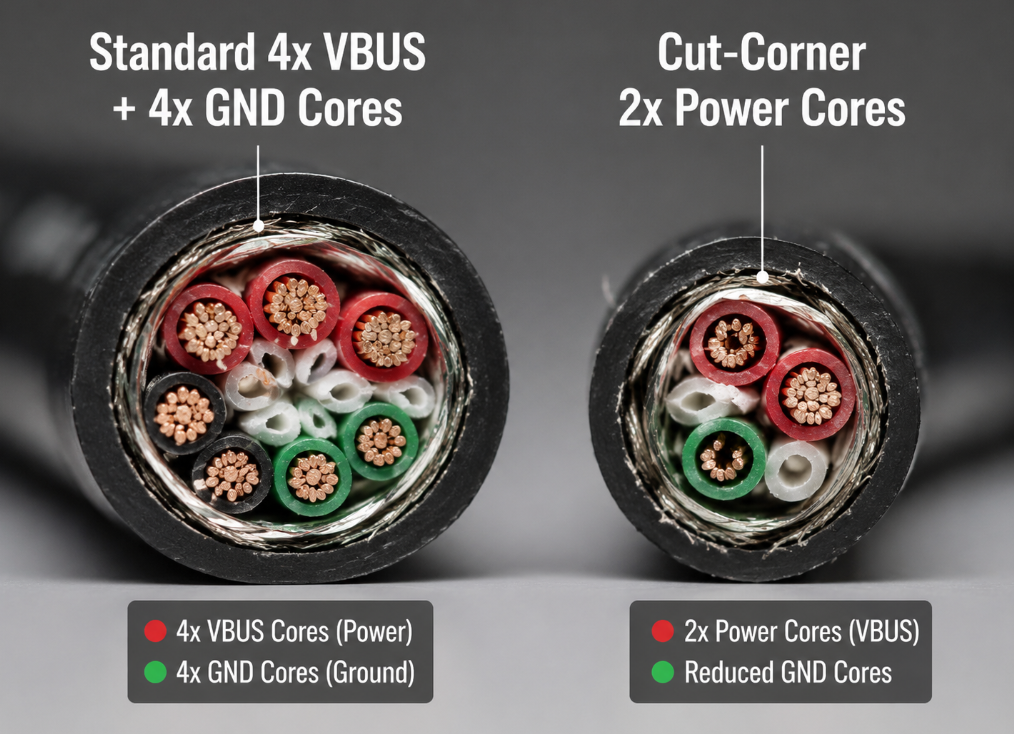
A special reminder here: USB-C is just an interface form, and does not directly equal high-power fast charging capability. To judge whether fast charging is possible, you need to look at internal contacts, cable specifications, protocol support, and certification, not just the appearance.
Also note that the pin shapes of USB-C plugs (male) and sockets (female) are different: one is an exposed contact, the other is an internal shrapnel, but the pairing logic is the same — only when the charger, cable, and device interface all support the corresponding current level can the nominal power be stably fully utilized, and any cut corner in any link will hold back performance.
Electrical Logic of VBUS: Voltage, Current, and Negotiation
Many people think that VBUS itself can output various voltages, but that is not the case. It is just a “wire”, and the voltage and current are determined by the devices at both ends and protocol negotiation.
Common Voltage Levels
The VBUS voltage of USB-C is not fixed, ranging from the lowest 5V to the highest 48V, with different levels corresponding to different power ranges:
| Voltage Level | Protocol Range | Common Capability Range | Typical Applications |
|---|---|---|---|
| 5V | Default power supply level for all USB-C connections | Several hundred mA ~ 3A, higher current requires additional cable and protocol support | Basic charging, device connection identification |
| 9V/12V/15V/20V | USB PD standard power fast charging | Up to 100W (20V 5A) | Fast charging for mobile phones, tablets, thin and light laptops |
| 28V/36V/48V | USB PD extended power range | Up to 240W (48V 5A) | Gaming laptops, high-power monitors, professional peripherals |
Note: Among PD standard power levels, 12V is not a mandatory support level for all devices, and the actual negotiation result shall prevail.
In a compliant Type-C/PD process, the source end usually provides 5V default VBUS first after the connection is confirmed, and then negotiates to enter a higher voltage through the CC pin; however, whether there is continuous 5V output depends on the device role, connection status, and the product’s power management strategy. This staged voltage boost design is to ensure compatibility and safety.
Determinants of Voltage and Current
The voltage of VBUS is not generated by itself, and is completely controlled by the power supply end (source end) according to the negotiation result. To reach a certain voltage level, three conditions must be met: “charger support, device support, cable support”, none of which can be missing. For example, if you use a 65W PD charger to charge a mobile phone that only supports 18W, the maximum output will only be 9V 2A, and it will not force 65W into it.
The upper limit of current is jointly determined by four factors: first, the rated output capacity of the charger; second, the maximum input demand of the device; third, the rated current of the cable (for example, a 3A cable can run up to 60W, a 5A cable can run 100W, and cables exceeding 3A generally have a built-in e-marker chip to indicate their capability); fourth, the resistance on the path — including the contact resistance of the contacts, the copper core cross-sectional area of the cable, and the cable length. The greater the resistance, the lower the current that can be carried, and the more severe the heat generation.
Common Abnormalities and Safety Mechanisms
The most common abnormality in daily use is “only 5V charging, no fast charging”. Nine times out of ten, this is a negotiation failure: it may be that the CC pin of the cable is broken, the cable does not support the corresponding PD level, or the device or charger is incompatible. If low-power charging is normal, but high-power use causes heat, speed drop, or even charging interruption, then the first suspect is that the carrying capacity of the cable or interface is insufficient.
In terms of safety, USB power supply has multiple protections: staged control starting with default 5V and boosting only after negotiation, and the source end generally has over-current, over-voltage, short-circuit, and over-temperature protection. But this does not mean that “default 5V is absolutely safe” — although 5V will not electrocute people, the current during a short circuit can reach several amps or even more than ten amps, which is enough to burn out cables, interfaces, and even cause fire risks. You should still pay attention to avoiding metal foreign objects short-circuiting the interface.
Functions of GND: Return, Reference, and Anti-Interference
Many people only value VBUS and think that GND is just “a ground wire” and not that important. In fact, the quality of GND directly affects power supply stability and can even interfere with data transmission.
Three Core Functions
The first function of GND is the current return path — current flows from VBUS to the chips and battery in the device, and after completing its work, it must return to the power supply end through GND to form a complete closed loop. Without GND, current cannot flow at all.
The second function is the voltage reference baseline — the 5V and 9V we refer to are the voltage difference of VBUS relative to GND. If GND is unstable, voltage measurement is meaningless, and the device’s circuit cannot work normally, just like measuring mountain height requires a sea level baseline first.
The third function is to reduce noise and crosstalk — GND is a common low-impedance channel in the circuit, and all kinds of clutter and electromagnetic interference can be conducted away through GND, reducing interference to data signals.
Why GND Also Uses a Multi-Pin Design
GND and VBUS are paired. Since VBUS uses multiple pins in parallel, GND also needs a corresponding number of pins: on the one hand, it can form a symmetrical return path with VBUS, reducing the total return impedance, voltage drop, and heat generation; on the other hand, multiple pins can also improve stability after plugging and unplugging wear, avoiding poor GND contact caused by oxidation of a single contact.
Differences Between GND, Chassis Ground, and Shielding Layer
This is the most easily confused point: GND in the circuit is the “working ground”, responsible for current return and voltage reference; chassis ground and shielding layer are “protective ground/shielding ground”, responsible for blocking electromagnetic interference and discharging static electricity.
In mass-produced products, the two are usually connected through 0-ohm resistors, capacitors, or other controlled devices, rather than directly short-circuited — if directly connected, static electricity may directly enter the circuit and burn out the chip, and may also form a ground loop, which instead increases interference. Simply put, the shielding layer is the “protective layer”, and GND is the “working line”. The two are related but not the same thing.
Manifestations of GND Abnormalities
When GND has problems, the symptoms are often not just slow charging: for example, power supply level drop, obvious interface heating, large voltage drop; unstable data transmission, frequent bit errors or even disconnection; some touch-enabled devices may also experience touch jumping or automatic restart during charging. These may all be caused by poor GND contact or too high return impedance.
Wiring and Selection: Key Points from PCB to Cable
Whether it is the circuit board wiring inside the device or the external cable selection, the design of VBUS and GND is the core, which directly determines whether the power supply can stably reach full power.
Basic Idea of Power Supply Path
After VBUS enters from the interface, it cannot be directly connected to the battery or load. It must first pass through protection devices, and then be connected to the power management chip, charging chip, or load switch — this way, once over-current or over-voltage occurs, the protection devices will act first, and will not burn out the subsequent core circuit. The core of GND design is three words: low, short, straight — low impedance, short path, as few turns as possible, and do not allow a slender “bottleneck” on the high-current return path, otherwise the bottleneck will generate serious heat.
Core Concerns of PCB Wiring
If you are doing circuit board design, there are several key points to note: first, the line width, copper thickness, and number of vias should match the target current. The larger the current, the thicker the line, the thicker the copper, and the more vias should be drilled to avoid vias becoming a bottleneck; second, VBUS and GND should be planned in pairs as much as possible. For example, if VBUS runs on the top layer, GND runs on the corresponding position on the bottom layer, so that the return path is the shortest and interference is minimal; third, there should be no necks or acute angles in high-current areas, and do not drill too many vias, as these will increase resistance and heat generation; fourth, more copper should be poured near the connector pads, which can both dissipate heat and improve mechanical strength, preventing the pads from falling off after long-term use of the interface.
Indispensable Protection Devices
Several types of protection devices are generally required on the VBUS path: over-current protection (such as fuses, which blow when the current is too large to protect the subsequent circuit), TVS/ESD protection (used to discharge static electricity, for example, the high-voltage static electricity from touching the interface in winter will be conducted away and will not burn the chip), reverse current protection (to prevent current from the device end from flowing back to the power supply end, for example, when a power bank charges a mobile phone, the mobile phone will not charge the power bank in reverse). Some designs also add a VBUS discharge circuit to quickly discharge residual power after unplugging the power supply, avoiding abnormalities caused by residual voltage.
Selection of Cables and Adapters
Ordinary users are most likely to encounter pitfalls with cables. The logic for selecting cables is the same as for interfaces: don’t just look at the appearance, focus on several core parameters: rated current, length, whether there is official certification, and whether there is an e-marker chip. For cables with the same rated current, the shorter the cable and the thicker the copper core, the smaller the voltage drop and the lower the heat generation; thin cables, long cables, and low-quality terminals will amplify voltage drop and temperature rise, and are prone to level drops or even damage in high-power scenarios. The same goes for adapters: low-quality products may only have half of the pins connected, and cannot run high power at all.
Grounding Strategy for Chassis and Shielding
The connection between the shielding layer and the circuit GND must take into account both ESD (electrostatic discharge protection) and EMI (electromagnetic interference) requirements: static-sensitive products are often connected through RC circuits, which can both discharge static electricity and block low-frequency interference; metal shell devices may be directly connected, but it is necessary to avoid forming ground loops that introduce noise. Remember not to use the shielding layer directly as the power return GND.
Detection and Troubleshooting: How to Judge If There Is a Problem with VBUS/GND
When encountering problems such as slow charging, heat generation, or disconnection, there is no need to rush to send it for repair. Troubleshoot in order from easy to difficult, and you can find the cause of most problems by yourself.
Preliminary Judgment Without Tools
If there are situations such as slow charging, obvious interface heating, repeated charging disconnection, or only low-power charging, first find a confirmed qualified cable (such as an original cable, an officially certified cable) and replace it to try — if it returns to normal immediately after changing the cable, then it is basically a problem with the original cable or terminal. If the same device and the same charger have very different charging speeds with different cables, first suspect the cable specification, plug terminal status, or poor contact; if there are still differences after replacing multiple qualified cables, then troubleshoot the device port, charger compatibility, or the device’s own temperature control strategy.
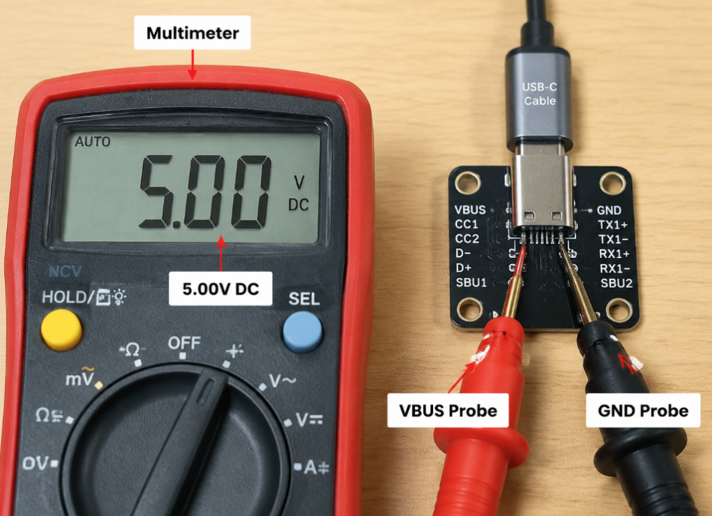
Basic Measurement with a Multimeter
If you have a multimeter, you can do several simple measurements: first, measure the no-load voltage of VBUS to GND, which usually has a 5V default voltage after normal connection; you can also measure the voltage drop across the cable under full load — for example, under 5V output, if the voltage at the other end of the cable drops below 4.5V under full load, it means the cable’s resistance is too large and its carrying capacity is insufficient; you can also measure the continuity at both ends of the cable to determine if there are broken pins.
It should be noted that ordinary multimeters can only verify the actual voltage and conduction voltage drop of VBUS to GND, and cannot parse the details of PD negotiation messages; to accurately judge whether the PD level is triggered, it is best to use test tools with PD protocol display, or measure under the loaded state of the device’s normal charging — some devices will not boost voltage when no-load, when the load is not triggered, or when a PD contract is not established, and only measuring no-load voltage may not show the high-voltage level.
Priority Order of Troubleshooting
Troubleshooting power supply problems must be done from easy to difficult to avoid detours: the first step is to replace with a qualified cable, after all, cables are the most prone to problems and the easiest to replace; the second step is to try a different charger or a different power supply port to rule out problems with the power supply end; the third step is to check the device’s USB-C interface to see if there is dust, oxidation, or shrapnel deformation, which will cause the contact resistance to increase. Wiping with an alcohol cotton pad and cleaning the dust may fix it; if all of the above are fine, then consider that there is a fault in the internal power supply path or protection device of the device, and it is not too late to send it for repair at that time.
Corresponding Causes of Common Symptoms
There are several common symptoms that can quickly locate the problem: if only 5V can be output and fast charging is not possible, it is mostly a protocol negotiation or compatibility problem, such as the cable not supporting PD, or the CC pin being broken; if the interface or cable is obviously hot, it is mostly due to too large contact resistance, insufficient cable carrying capacity, or too few effective pins on the interface; if data transmission is slow and frequently disconnected, it is not necessarily a problem with VBUS. You should also check whether GND has poor contact, whether there is a problem with the shielding layer, and even the status of the data pins themselves.
Common Misconceptions and Boundary Conditions
Regarding VBUS and GND, there are several widely circulated wrong statements, which we will correct all at once here.
The first misconception is “the more VBUS pins, the greater the power”. In fact, the number of pins is only the foundation, just like more water pipe joints do not mean a larger total flow. It also depends on the carrying capacity of each pin, the thickness of the cable’s copper core, the rated current of the connector, and the result of protocol negotiation. Even if there are 4 VBUS pins, if the cable only has a 0.5 mm² copper core, it cannot carry high current.
The second misconception is “it doesn’t matter if there are fewer GND pins”. Many low-quality cables cut corners and only connect 2 GND pins, thinking that since it’s just ground, missing two is fine — in fact, insufficient GND will directly increase the return impedance, leading to increased heat generation and voltage drop, and even affect data transmission due to unstable reference. The harm is no less than missing VBUS pins.
The third misconception is “default 5V is absolutely safe”. 5V is indeed a low voltage and will not electrocute people, but the current during a short circuit can be very large, enough to burn out cables, interfaces, and even cause fires; in addition, if the PD negotiation circuit has a problem, abnormal voltage boost may also occur, so you should still be careful not to poke the interface with metal foreign objects, and do not use low-quality chargers.
The fourth misconception is “only one side of the pins works when plugged in either way”. Many people think that USB-C reversible plugging is just “it works”, and only the pins on one side are supplying power. In fact, in a compliant USB-C design, the corresponding VBUS and GND pins on both upper and lower sides will conduct when plugged in either way, sharing the current together, and there is no situation of “only one side working”.
The fifth misconception is “all USB-C cables support fast charging”. USB-C is just an interface form, and fast charging capability is determined by the cable’s rated parameters, e-marker, and certification, and cannot be judged solely by appearance.
Practical Reference: Reverse Engineering Design and Cable Selection from Requirements
Different usage scenarios have different requirements for VBUS and GND. We can start from actual needs to determine how to select cables and how to design.
For example, ordinary mobile phone charging is generally around 5V 2A, with low power. At this time, the focus is on contact reliability and basic conductivity. There is no need to deliberately pursue high-end cables of several hundred watts, as long as they are qualified cables from regular manufacturers. Of course, using high-end cables is also fine, just a bit wasteful.
If it is a laptop fast charging of around 65W, the common specification is 20V 3.25A, which has exceeded the standard capability upper limit of ordinary 3A cables; to stably run full 65W, you should usually choose qualified cables with a rated 5A and e-marker chip. If you only use a 3A cable, usually you can only negotiate up to 60W, or run at a reduced level, and the cable and interface are more prone to heat generation during charging.
For high-power devices from 100W to 240W, such as gaming laptops and mobile workstations, the requirements are even higher: cables that support the corresponding PD version, with e-marker chips, and rated current that meets the standard are required. At the same time, the heat dissipation design of the cable and interface must also be in place, otherwise it is easy to trigger protection due to overheating, lose power, and even have safety hazards.
There is another common scenario: the device only needs charging and does not need data transmission. Many people think that since data is not used, it’s fine to connect fewer pins, and even some manufacturers deliberately reduce the number of VBUS and GND pins to save costs. In fact, even if only for charging, it is necessary to ensure that the number of VBUS and GND pins and cable specifications meet the power requirements. Otherwise, the risk of heat generation and interface burnout under high current will be much higher, and “pin reduction” cannot be used as a universal cost-saving measure.
In general, VBUS and GND are the foundation of USB-C power supply, and neither is dispensable. When encountering power-related problems, there is no need to rush to conclusions. First confirm whether you are using a standard USB-C solution or a simplified version, then check whether the voltage and current of VBUS can meet the requirements, whether the GND return path has sufficiently low impedance, and whether the cable and internal wiring are designed according to the corresponding power. Finally, troubleshoot step by step combined with the symptoms, and the cause of most problems can be found. Whether you are an ordinary user selecting cables or a beginner doing wiring design, understanding the logic of these two groups of pins will help you avoid the vast majority of USB-C power supply pitfalls.