
Quick Summary
Burn-in testing is a standardized reliability screening process that runs electronic products under controlled elevated stress conditions before shipment. By combining high temperature, calibrated electrical load, and extended runtime, it accelerates the appearance of hidden “infant mortality” defects and removes faulty units before they reach customers.
This guide covers everything you need to know:
- Core definition and real-world value of burn-in testing
- The bathtub curve theory behind early product failures
- Common test types including HTOL, HAST, and dynamic burn-in
- Step-by-step test workflow and key parameters
- Real-world example with USB-C and GaN fast chargers
- Global industry standards from JEDEC, AEC-Q, and IEC
- Common misconceptions and frequently asked questions
1. What Is Burn-In Testing?
1.1 Core Definition: A “Stress Physical” for Electronics
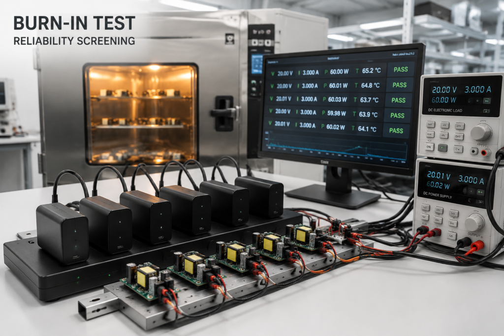
Burn-in testing (also called aging test) is a production-level quality control process where electronic components or finished devices operate continuously under controlled stress conditions. Think of it as a rigorous medical checkup for electronics: instead of just verifying “it works right now,” it pushes products to expose hidden weaknesses that would otherwise fail weeks or months after delivery.
Per JEDEC JESD22-A108, the global semiconductor standard, burn-in is a short-duration high-temperature bias life test specifically designed to screen for infant mortality-related failures.
1.2 Core Purpose: Filter Out Hidden Factory Defects
The primary goal of burn-in is not to test maximum lifespan, but to eliminate early-life failures. It catches defects that standard 30-second functional tests will never find, ensuring every shipped unit enters the stable, low-failure phase of its lifecycle.
1.3 Where Burn-In Sits in the Production Line
Burn-in testing takes place after assembly and initial functional testing, and before final packaging and shipment:
R&D Validation → Pilot Production → Assembly → Functional Test → Burn-In Testing → Final Inspection → Shipment
1.4 Why Burn-In Matters for Both Brands and Buyers
- Reduces field failure rates by 60–80% for high-reliability products
- Cuts warranty repair costs and brand reputation damage
- Improves batch-to-batch performance consistency
- Meets mandatory supply chain requirements for automotive, medical, and aerospace industries
2. The Bathtub Curve: Why Early Failures Happen
2.1 The Three Phases of Product Lifecycle
Reliability engineers use the “bathtub curve” to describe how product failure rates change over time. This U-shaped pattern is the foundational logic behind all burn-in testing:
- Infant Mortality Phase: High initial failure rate caused by manufacturing defects and material weaknesses. Failure rate drops rapidly as weak units fail.
- Useful Life Phase: Low, stable random failure rate. This is the normal service life of a well-built product.
- Wear-Out Phase: Failure rate rises again as components reach their natural end of life due to material aging.
2.2 Burn-In Targets Only the First Phase
Burn-in testing operates exclusively on the left side of the bathtub curve. By simulating weeks or months of use in just a few hours, it forces defective units to fail inside the factory instead of in the customer’s hands. Surviving units enter the stable useful-life phase before they are ever shipped.
2.3 What Causes Early Failures?
Most early failures stem from process imperfections, not design flaws:
- Impurities in semiconductor materials
- Solder joint defects (cold joints, voids)
- Component parameter deviations
- PCB contamination or assembly errors
- Insufficient thermal design margins
3. Core Principles: How Burn-In Accelerates Defect Detection
3.1 The Basic Idea of Accelerated Aging
Burn-in works on a simple principle: under controlled higher stress, defects that would take months to appear in normal use show up in hours. It is like fast-forwarding the product’s life without damaging healthy units.
3.2 Thermal Acceleration: The Arrhenius Effect
Temperature is the most powerful acceleration factor. Following the Arrhenius principle, chemical reaction and degradation rates roughly double with every 10°C rise in temperature. This is why elevated temperature is the backbone of nearly all burn-in programs.
3.3 Electrical Stress: Bias & Load Simulation
Electrical stress uses calibrated voltage bias and sustained high load to mimic long-term operation:
- Voltage bias applies slightly elevated supply voltage to stress insulation and semiconductor junctions
- Full-load operation runs the device at maximum rated power to generate maximum internal heat
- For consumer products, stress levels are typically 10–20% above nominal ratings, not extreme “high voltage” abuse
3.4 Thermomechanical Stress
Repeated heating and cooling causes materials to expand and contract at different rates (coefficient of thermal expansion mismatch). This exposes weak solder joints, PCB cracks, and package delamination that would fail after months of real-world thermal cycling.
3.5 Multi-Stress Synergy
The strongest screening effect comes from combining temperature, electrical load, and sometimes humidity. Together, they activate more failure mechanisms than any single stress alone.
4. Common Types of Burn-In Testing Methods
4.1 By Operating State
- Static Burn-In: Devices receive power bias but run no active functions. Simple, low-cost, and ideal for basic components and passive parts, but limited in defect coverage.
- Dynamic Burn-In: Devices run full functional workloads during stress. For example, a CPU runs maximum-load code, or a charger runs at full power. It catches function-related defects and is the standard for complex ICs and finished products.
4.2 By Stress Combination
- High Temperature Operating Life (HTOL): The most common burn-in method, combining high ambient temperature with continuous powered operation. Standard for semiconductor and general electronics reliability screening.
- Highly Accelerated Stress Test (HAST): Combines high temperature, high humidity, and voltage bias. It specifically detects moisture-related failures such as corrosion, ionic migration, and seal leaks, and replaces older slower temperature-humidity bias tests.
- Voltage Bias Burn-In: Focuses on electrical stress to detect gate oxide breakdown and insulation weaknesses in semiconductors.
- Thermal Cycling Burn-In: Alternates between high and low temperatures to test mechanical reliability of solder joints and assemblies.
- Multi-Stress Combined Burn-In: Adds vibration, power cycling, or other variables to closely match real-world operating environments.
4.3 By Test Object Level
- Component-Level Burn-In: Tests individual ICs, MOSFETs, capacitors, and other parts before assembly.
- Board-Level (PCBA) Burn-In: Tests fully assembled circuit boards to catch soldering and assembly defects.
- System/Finished Product Burn-In: Tests complete end products such as chargers, laptops, or industrial controllers.
- Wafer-Level Burn-In (WLBI): Performed on silicon wafers before packaging, reducing cost by catching defects early in semiconductor manufacturing.
5. Key Test Parameters: Temperature, Voltage, Load & Duration
5.1 Temperature Settings by Product Grade
| Product Grade | Typical Burn-In Temperature | Common Use Case |
|---|---|---|
| Consumer electronics | 60–85°C | Phone chargers, everyday gadgets |
| Industrial electronics | 85–105°C | Factory automation, power supplies |
| Automotive grade | 125–150°C | Under-hood electronics, ECUs |
| Aerospace / military | 125–150°C+ | Mission-critical systems |
5.2 Test Duration
Test length is calibrated to match product reliability requirements:
- Consumer chargers and small electronics: 2–8 hours
- Mid-range consumer and industrial products: 24–48 hours
- Industrial power and communication equipment: 48–72 hours
- Automotive and high-reliability devices: 168 hours (7 days) or longer
Longer test times provide more screening confidence, but follow diminishing returns.
5.3 Electrical Parameters
- Load level: Typically 100% rated load, sometimes 110–120% for accelerated screening
- Voltage bias: 1.0–1.2x rated voltage for most products; up to 1.5x for specific semiconductor screening
- Power cycling: Repeated on/off cycles to test startup reliability and thermal fatigue
5.4 Monitored Parameters During Testing
- Output voltage and current stability
- Power consumption and efficiency
- Case and internal component temperature
- Fault events and protection triggers
- Runtime parameter drift
5.5 Core Parameter Setting Principles
- Stress levels must be high enough to accelerate defects, but low enough not to damage healthy products
- Settings must align with industry standards and product material limits
- Duration is balanced between screening effectiveness and production cost
6. Step-by-Step: A Full Burn-In Test Workflow
6.1 Preparation Phase
- Test plan definition: Match stress levels, duration, and pass/fail criteria to product grade and applicable standards
- Baseline measurement: Record initial electrical parameters and functional status of all samples at room temperature
- Equipment calibration: Verify temperature chambers, power supplies, and data loggers are calibrated and accurate
6.2 Execution Phase
- Sample loading: Secure units in test fixtures and verify electrical connections
- Gradual ramp-up: Step up temperature and load slowly to avoid thermal or electrical shock damage
- Continuous monitoring: Log voltage, current, and temperature at set intervals; trigger alarms for anomalies
- Event logging: Record all faults, shutdowns, and parameter deviations with timestamps
6.3 Post-Test & Analysis Phase
- Gradual recovery: Ramp down temperature and load, then let units stabilize at room temperature
- Post-test verification: Re-run full functional and electrical tests to compare against baseline values
- Failure analysis: Investigate failed units to identify root cause — component defect, solder issue, or design weakness
- Reporting: Issue pass/fail determination, batch failure rate statistics, and process improvement recommendations
7. Core Equipment for Burn-In Testing
7.1 Environmental Stress Unit: Burn-In Chamber / Oven
A temperature-controlled chamber with forced air circulation provides uniform thermal stress. Quality units maintain temperature accuracy within ±2°C and support programmable ramp/soak profiles.
7.2 Electrical Stress Units: Programmable Power Supplies & Electronic Loads
- Programmable power supplies: Deliver precise, adjustable input voltage and bias conditions
- Electronic loads: Simulate real-world output load in constant-current, constant-voltage, or constant-power modes
7.3 Data Acquisition & Monitoring System
Centralized software tracks every test channel in real time, logs historical data, triggers automatic alarms, and generates compliance reports.
7.4 Test Fixtures & Burn-In Boards
Custom PCBs and sockets provide reliable electrical connection to dozens or hundreds of units simultaneously, with built-in power distribution and sensing.
7.5 Temperature Measurement Tools
Thermocouples, infrared sensors, and thermal imagers monitor case temperature, PCB hotspots, and component junction temperatures.
8. Hidden Defects Detected by Burn-In Testing
8.1 Component-Level Failures
- Electrolytic capacitor ESR drift and early degradation
- MOSFET and semiconductor thermal breakdown
- IC threshold voltage shift and parametric drift
- Internal bond wire weakness
8.2 Manufacturing & Assembly Defects
- Cold solder joints and solder voids
- Solder crack propagation under thermal stress
- PCB ionic contamination causing leakage
- Flux residue and cleaning defects
8.3 Thermal Design Issues
- Insufficient heat dissipation leading to overheating
- Hotspot locations missed in prototype testing
- Thermal interface material gaps or voids
8.4 Electrical Performance Anomalies
- Output voltage instability under sustained load
- Excessive ripple and noise growth
- Protection circuit false triggering
- Insulation leakage under high temperature
8.5 Structural Reliability Risks
- PCB delamination and via cracking
- Package layer separation
- Connector contact degradation
9. Real-World Example: USB-C & GaN Charger Burn-In Process
9.1 Why Fast Chargers Require Burn-In
Modern GaN chargers run at higher switching speeds and power densities than traditional silicon chargers, creating higher internal thermal stress. Un-tested GaN chargers can have a 5–10% dead-on-arrival (DOA) rate in the field. Burn-in is the single most effective step to eliminate this early failure risk.
9.2 Typical Test Setup
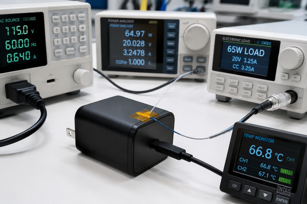
- Test subjects: 20W USB-C chargers, 65W GaN chargers, 140W PD 3.1 chargers
- Test chain: AC source → power analyzer → USB-C electronic load → temperature monitoring
- Standard duration: 4–12 hours depending on power rating and quality tier
9.3 Core Test Items
- Full-load burn-in: Continuous maximum power output (e.g., 20V × 3.25A for 65W units)
- Input voltage variation: 90V / 115V / 230V / 264V AC input range sweep
- Dynamic load cycling: Simulate real charging patterns from idle to full power
- Power on/off cycling: Repeated startup to test control IC stability
9.4 Key Monitored Metrics
- Output voltage accuracy and stability
- Charging efficiency over time
- Case and internal hotspot temperature
- Output ripple and noise levels
- PD protocol handshake stability
9.5 Pass Criteria
A charger passes burn-in if it maintains stable output, triggers no unexpected protection, stays within temperature limits, and shows no parameter drift outside specification after testing.
10. Industry Standards for Burn-In Testing
10.1 Semiconductor Industry Standards
- JEDEC JESD22-A108: The global baseline standard for temperature, bias, and operating life testing for integrated circuits; defines burn-in as a screening method for infant mortality
- JEDEC JESD47: Overarching standard for stress-test driven qualification of integrated circuits
10.2 Automotive Industry Standards
- AEC-Q100: Stress test qualification for automotive integrated circuits; includes HTOL burn-in requirements for different temperature grades (Grade 0 to Grade 3)
- AEC-Q101: Equivalent standard for discrete semiconductor devices
- AEC-Q200: Standard for passive automotive components
Note: AEC-Q standards are widely required automotive supply chain qualifications, not legal mandates.
10.3 General Electronics Environmental Standards
- IEC 60068 series: International standard for environmental testing of electronic equipment, including high-temperature and temperature-cycle test methods
10.4 Military & High-Reliability Standards
- MIL-STD-883 Method 1015: United States military standard for microcircuit burn-in testing, used for aerospace and defense electronics
11. How to Interpret Burn-In Test Results
11.1 Pass/Fail Determination
A unit passes burn-in testing when:
- All functions work normally after stress
- Key electrical parameters remain within datasheet specifications
- No visible damage, discoloration, deformation, or component bulging
- No intermittent or temperature-dependent faults appear
11.2 Failure Mode Classification
- Catastrophic failure: Complete loss of function, short circuit, or open circuit
- Parametric drift: Electrical parameters shift beyond acceptable limits
- Intermittent failure: Faults that appear and disappear with temperature, the hardest type to catch without burn-in
11.3 Batch Quality Analysis
- Batch failure rate: Percentage of failed units in the test batch, compared against historical baselines
- Weibull analysis: Statistical method to analyze failure trends and predict field reliability
- Root cause feedback: Failed units are analyzed to drive improvements in components, assembly, or design
12. Burn-In vs. Other Reliability Tests
12.1 Burn-In vs. Standard Functional Test
| Aspect | Functional Test | Burn-In Test |
|---|---|---|
| Duration | Seconds to minutes | Hours to days |
| Goal | Verify the product works | Verify long-term reliability |
| Load | Nominal operating conditions | Elevated stress conditions |
| Environment | Room temperature | High temperature / humidity |
| Defects found | Obvious broken units | Hidden early-life defects |
12.2 Burn-In vs. Temperature Cycling Test
Burn-in focuses on long-term electrical and thermal stability at sustained high temperature. Temperature cycling focuses on mechanical fatigue from expansion and contraction between extreme hot and cold.
12.3 Burn-In vs. Lifetime Testing
Burn-in is a short screening step for manufacturing defects. Lifetime testing evaluates total product lifespan over thousands of hours, and is used for design validation, not production screening.
12.4 Burn-In vs. Environmental Stress Screening (ESS)
ESS is a broader category that includes temperature cycling, vibration, and shock. Burn-in is one specific type of ESS focused on electrical and thermal stress over time.
12.5 Related Concepts: HALT & HASS
- HALT (Highly Accelerated Life Test): Ramps stress to destruction to find design limits and weaknesses, used in R&D
- HASS (Highly Accelerated Stress Screening): Production screening derived from HALT results, using higher stress than traditional burn-in for faster detection
13. Common Misconceptions & Frequently Asked Questions
13.1 Common Misconceptions
- Myth 1: Longer burn-in always means better reliability Beyond a certain point, extra test time adds little screening benefit but significantly increases cost and production lead time.
- Myth 2: Higher temperature always improves screening Excessive temperature damages perfectly good units and creates new failures that would never occur in real use. Optimal temperature balances detection strength and product safety.
- Myth 3: Passing burn-in means the product will never fail Burn-in removes most early-life defects, but cannot eliminate random failures or prevent end-of-life wear-out.
- Myth 4: All electronics must have burn-in testing Burn-in is a cost-benefit decision. Low-cost, low-risk consumer products may skip it, while automotive, medical, and aerospace products require it.
13.2 Frequently Asked Questions
Q: Does burn-in testing reduce the product’s normal service life?
A: Burn-in consumes a very small portion of the product’s total life margin, but its purpose is to remove defective units, not to wear out good ones. Properly calibrated burn-in has negligible impact on the usable life of a healthy product.
Q: Is running stress tests on my PC at home the same as factory burn-in?
A: Home “stress testing” of CPUs or GPUs is similar in concept, but factory burn-in uses calibrated temperature chambers, standardized load profiles, and controlled electrical conditions. Home testing validates one specific unit; factory burn-in is a batch quality control process.
Q: What is the main difference between consumer-grade and industrial-grade burn-in?
A: Industrial and automotive burn-in uses higher temperatures, longer durations, tighter parameter limits, and follows formal industry standards. Consumer burn-in is optimized for cost-effectiveness for lower-risk applications.
Q: How can I tell if a product went through proper burn-in testing?
A: Look for recognized certifications (CE, FCC, UL, IEC 60950), check for published reliability specifications such as MTBF, and consider brand reputation. Premium brands typically disclose their quality control processes.
Q: Why does burn-in make products more expensive?
A: Burn-in adds cost through equipment investment, test time, energy use, labor, and yield loss from removed defective units. However, it reduces warranty costs far more than it adds to production cost for quality-focused brands.
Q: Why do new electronics sometimes have a faint “new device” smell?
A: Mild initial odor comes from protective coatings, adhesives, and plastic components releasing trace volatile compounds during first use. This is normal and typically fades quickly. Proper burn-in can help reduce this initial outgassing before shipment.
14. Future Trends: Smart Burn-In Technology
14.1 Wafer-Level Burn-In Adoption
Moving burn-in earlier to the wafer stage reduces packaging and testing costs, and is becoming standard for advanced semiconductor nodes.
14.2 AI-Powered Adaptive Burn-In
Machine learning algorithms analyze real-time test data to dynamically adjust stress levels. This reduces total test time while maintaining or improving screening effectiveness.
14.3 Real-Time Monitoring & Predictive Screening
IoT sensors and cloud analytics enable early failure prediction, so failing units can be removed from the test early instead of waiting for the full cycle.
14.4 Automated & Digital Test Lines
Fully automated loading, monitoring, and reporting systems improve consistency, reduce human error, and provide complete digital traceability for every tested unit.
15. Final Thoughts
Burn-in testing is the unsung gatekeeper of electronics quality. It is the reason a well-built charger, laptop, or car control unit works reliably day after day instead of failing unexpectedly after a few weeks.
For manufacturers, the best burn-in strategy is never “the longest” or “the hottest” — it is the one calibrated to the product’s risk level, aligned with industry standards, and balanced between quality assurance and production efficiency.
For consumers, choosing products from brands that invest in proper burn-in and reliability testing is one of the most reliable ways to avoid frustrating early failures and get better long-term value.