
Quick Summary
- Gallium Nitride (GaN) is an advanced semiconductor material that converts and controls electrical power more efficiently, especially in high-frequency power applications
- It is best known for compact fast chargers, and is also widely deployed in data centers, electric vehicles, telecommunications and renewable energy systems
- Its core value lies in delivering smaller size, lower heat generation and higher energy efficiency at the same power rating
Why GaN Chargers Have Suddenly Become Popular
Traditional 65W laptop chargers are bulky and inconvenient to carry, and bringing separate chargers for phones, tablets and laptops adds heavy travel baggage. A multi-port 65W GaN charger with USB-C PD can power all three devices at once, and is significantly more portable than equivalent silicon-based models. Driven by widespread USB-C PD adoption and mature 650V GaN-on-Si technology for consumer use, 30W to 140W GaN chargers have become a premium standard in consumer electronics.
What Exactly Is GaN?
Basic Definition
Gallium Nitride (GaN) is a compound semiconductor made of gallium (Ga) and nitrogen (N), and a core representative of wide-bandgap (WBG) semiconductors. Compared with traditional silicon, it is far better suited for handling high-voltage and high-frequency power.
The Semiconductor Family
Traditional silicon (Si) remains mature, low-cost and dominant in low-voltage, low-frequency scenarios, while wide-bandgap materials such as GaN and SiC withstand higher voltage and temperature, switch faster, and are important materials for next-generation power electronics.
Advanced Knowledge
It belongs to the III-V group of compound semiconductors, with the chemical formula GaN and a molar mass of 83.73 g/mol. Its primary crystal structure in commercial use is wurtzite, with zinc blende and rock salt as less common variants.
Why GaN Has Advantages Over Silicon in Power Applications
Faster Switching Speed
A semiconductor “switch” acts as an electronically controlled toggle that regulates current flow. GaN can switch current at much higher frequencies, which drastically reduces the size of surrounding passive components.
Lower Energy Loss
Far less electrical energy is wasted during the switching process, resulting in significantly reduced heat generation.
Higher Voltage Capability
It withstands higher voltage within the same chip area and delivers stronger current conduction per unit area.
System-Level Benefits
In well-optimized designs, overall system size and weight can be noticeably reduced, thermal design is simplified, and long-term energy consumption is lower.
Why GaN Makes Chargers Smaller
Core Logic: Switching Frequency Determines Passive Component Size
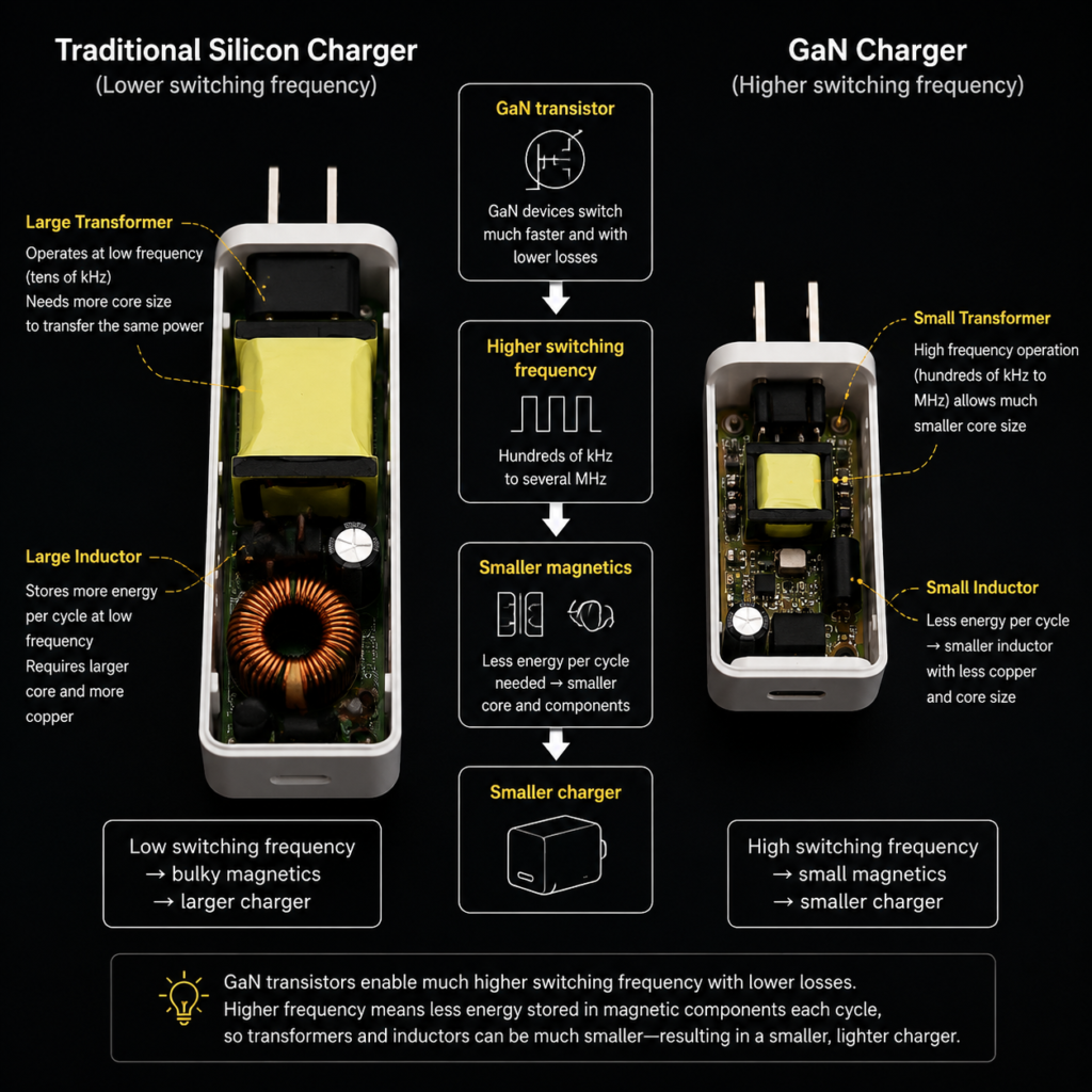
Traditional silicon-based chargers run at low switching frequencies, so they require large transformers and inductors for energy storage and filtering.
GaN chargers operate at drastically higher frequencies, which allows smaller magnetic components and reduces the size requirements of surrounding inductors and capacitors.
The Reduction Chain
GaN device → higher switching frequency → smaller magnetic components → smaller inductors and capacitors → smaller charger
How GaN Works
Core Principle: 2DEG (Two-Dimensional Electron Gas)
2DEG is a high-speed electron transport layer inside the material, simply understood as an “electron highway” where electrons move with very little resistance, enabling extremely fast switching and low conduction losses.
Main Device: GaN HEMT Transistors
Consumer fast chargers generally use enhancement-mode (normally-off) devices. They conduct when positive voltage is applied and turn off when voltage is removed, similar to a standard normally-off switch for safe operation.
Advanced Knowledge
- Depletion-mode (D-mode): normally-on, requires negative voltage to turn off
- MIS-HEMT: insulated-gate structure with lower gate leakage
- Vertical GaN: targeted at high-voltage high-power applications, still under development
- Integrated GaN power IC: monolithically integrated driver, protection and power transistor
Core Performance Comparison
Basic Feature Comparison
| Feature | GaN | Silicon |
|---|---|---|
| Bandgap | ~3.4 eV | ~1.12 eV |
| Switching speed | Faster | Slower |
| Energy loss | Lower | Higher |
| Power density | Higher | Lower |
Why These Properties Matter
| Feature | Why it matters |
|---|---|
| Higher breakdown field | Handles higher voltage safely |
| Faster switching | Enables smaller power supplies |
| Lower losses | Produces less heat |
Technical Parameter Details
GaN has roughly 10 times the breakdown field strength and more than twice the electron saturation velocity of silicon, and GaN-based power solutions typically reach 94%–96% conversion efficiency.
Advanced: How GaN Chips Are Manufactured
- GaN-on-Si: lowest cost, mainstream for 6–8 inch mass production, the dominant solution for consumer fast chargers
- GaN-on-Sapphire: primarily used in LED manufacturing, with some RF applications
- GaN-on-SiC: excellent RF performance and thermal conductivity, mostly used in 5G base stations
- Free-Standing Bulk GaN Substrate: best overall performance, extremely high cost
Where GaN Is Actually Used Inside a Charger
Power Flow Path
Mains AC → rectification → power control → GaN power transistor → transformer → USB-C PD controller → device charging
Role of GaN
GaN primarily replaces the high-voltage switching transistor inside the charger. It does not make up the entire charger, but serves as the core component responsible for high-speed power switching.
GaN vs Silicon vs Silicon Carbide (SiC)
Positioning Differences
- Silicon: the cost-performance leader, still irreplaceable in low-voltage low-frequency scenarios
- GaN: optimized for high-frequency, high-efficiency switching at medium and low voltages
- SiC: the high-voltage workhorse, built for high-voltage high-power applications
GaN Strengths
It excels in medium-to-low voltage applications up to 650V at high frequencies, including consumer fast chargers, data center power supplies and 5G RF systems, with switching frequencies up to several MHz and higher power density.
SiC Strengths
It generally outperforms in high-voltage high-power applications above 600V, especially the 1200V class, such as EV main inverters and central photovoltaic inverters, thanks to higher thermal conductivity and better heat dissipation at high currents.
Summary
The three technologies complement rather than replace each other, each with its own optimal use cases.
Major Application Areas
Consumer Electronics
USB-C PD fast chargers for phones and laptops (30W–240W, with 65W/100W/140W as mainstream), power adapters for monitors, TVs and gaming consoles, and charging systems for drones and power tools.
Data Centers & Servers
High-efficiency AC-DC power modules, 48V bus conversion and point-of-load (POL) converters that reduce power loss, lower data center PUE and improve overall energy efficiency.
Automotive Electronics
On-board chargers (OBC), DC-DC converters, 48V mild-hybrid systems and LiDAR drivers. Selected automotive-grade GaN devices are undergoing reliability qualification and gradually entering production applications.
Industrial & Renewable Energy
Photovoltaic microinverters, power conversion systems (PCS), servo motor drives, uninterruptible power supplies (UPS), wireless power transfer and industrial robot motor drives.
RF & Communications
5G macro base station power amplifiers, satellite communications, phased-array radar, cable TV amplifiers and 6G terahertz communication research.
Optoelectronics
Blue/green and white LEDs, blue laser diodes, and ultraviolet LEDs for disinfection and water purification.
Global Industry Landscape
Upstream: Substrates & Epitaxy
Substrate and epitaxial materials define GaN performance and cost, and MOCVD systems are the core manufacturing equipment.
Midstream: Device Design & Manufacturing
Leading power GaN vendors include Infineon, Navitas Semiconductor, Texas Instruments, EPC and Innoscience. Key RF GaN players are Qorvo, Wolfspeed and MACOM. The industry follows both IDM and fabless business models.
Downstream: Systems & End Products
Power supply designers, consumer electronics brands and telecommunications equipment vendors.
Regional Distribution
The United States leads in RF GaN and power GaN innovation; Europe is strong in industrial and automotive-grade power devices; Japan has deep expertise in materials and substrates; China sees booming consumer fast-charger adoption and rapidly expanding production capacity.
Technical Challenges and Limitations
Material Level
Bulk single-crystal substrates remain difficult and expensive to manufacture. Heteroepitaxy suffers from lattice mismatch and stress, defect density is higher than in silicon devices, and thermal conductivity is lower than SiC, limiting high-power heat dissipation.
Device Level
Enhancement-mode (E-mode) fabrication is technically challenging, dynamic on-resistance (D-Ron) degradation persists, gate voltage margins are tight, high-voltage devices above 650V lack full maturity, and vertical GaN is not yet in large-scale commercial use.
System Level
High-frequency switching introduces greater EMI challenges, gate drive circuit design is more complex, package parasitics have a notable performance impact, and long-term reliability data is still being accumulated.
Market Level
Device costs remain higher than silicon MOSFETs, design engineer familiarity is still limited, and industry standards and test specifications continue to evolve.
Development Trends and Future Outlook
Technology Evolution
The industry is advancing from lateral to vertical GaN structures for higher voltage ratings, developing integrated GaN power ICs with built-in drivers and protection, adding smart sensing and diagnostics, scaling 8-inch GaN-on-Si mass production for lower costs, and researching diamond-substrate GaN for ultimate thermal performance.
Market Growth Directions
Consumer fast charger penetration will continue to rise, with 100W+ models becoming standard. Data center high-efficiency power supplies will accelerate silicon replacement, automotive OBC and DC-DC deployments will scale up, and photovoltaic and energy storage markets will open new growth avenues. Industry consensus points to strong double-digit growth for GaN power devices overall.
Strategic Significance
GaN supports global carbon neutrality and energy efficiency improvements, underpins 5G/6G communications infrastructure, is a key technology for defense electronics and radar systems, and represents an important semiconductor technology field in the post-Moore’s Law era.
Common Misconceptions Clarified
- Myth: GaN will completely replace silicon.
Fact: GaN complements and upgrades silicon; silicon retains significant cost advantages in low-voltage low-frequency scenarios. - Myth: Higher power GaN is always better.
Fact: GaN performs best in medium/low-voltage high-frequency applications; SiC is more suitable for ultra-high voltage. - Myth: All “GaN” chargers perform the same.
Fact: Control topology, device quality and thermal design vary widely, leading to large differences in efficiency and reliability. - Myth: GaN chargers produce zero heat.
Fact: GaN reduces losses but still generates heat; good thermal design remains essential. - Myth: Any GaN charger automatically charges faster.
Fact: Charging speed depends on output power, PD/PPS protocol support, cable rating and device compatibility; GaN is just one core component.