
Quick Summary
- Active Clamp Flyback (ACF) is an upgraded topology of the conventional flyback power supply, and one of the core technologies in today’s compact high-efficiency chargers.
- Its key improvement: replaces the passive RCD snubber with an active clamp branch made of a switch and a capacitor, to recover energy from transformer leakage inductance.
- It enables Zero-Voltage Switching (ZVS), boosts full-load efficiency by 3%–5%, and supports higher switching frequency and greater power density.
- It is widely used in GaN fast chargers for phones, laptop power adapters, and other products where small size and low heat are critical.
- Tradeoffs include higher circuit complexity, higher bill-of-materials cost, and a steeper design learning curve; it is mainly used in mid-to-high-end efficient charging products.
1. Introduction: Why Do Chargers Need Active Clamp Flyback?
If you have paid attention to chargers in recent years, you may have noticed a clear trend: a 65W or even 100W fast charger is now smaller than an old 10W phone charger, and runs much cooler.
This “double the power, halve the size” progress comes not only from new devices like GaN transistors, but also from upgrades in the underlying power supply topology — and Active Clamp Flyback is the most representative example.
1.1 Flyback Topology: The Mainstay of Low-Power Chargers
Inside every charger is a power circuit that converts high-voltage AC into low-voltage DC. Among all topologies, the flyback converter is the dominant choice for low-to-medium power isolated power supplies.
From phone chargers and USB-C PD adapters to small home appliance power supplies, most products use a flyback architecture. Its core advantages are straightforward: simple circuit structure, controllable cost, natural input-output galvanic isolation, and compatibility with a wide 85–265Vac global input range.
1.2 The Inherent Bottleneck of Conventional Flyback: Problems Caused by Leakage Inductance
While mature and reliable, the conventional flyback has a fundamental flaw — transformer leakage inductance.
You can think of a transformer as two coils that transfer energy via a magnetic field. Ideally, all energy from the primary side would couple to the secondary side. In reality, a small portion of the magnetic field never couples, creating a parasitic inductance called leakage inductance.
When the main switch turns off, the energy trapped in the leakage inductance has nowhere to go, forming a dangerous voltage spike. This spike does more than just stress components — it causes three major problems:
- Energy waste: Conventional designs use an RCD snubber (resistor + capacitor + diode) to dissipate all leakage energy as heat.
- High switching loss: In hard-switching mode, voltage and current overlap during switching transitions, causing significant losses.
- Strong electromagnetic interference: Steep voltage transitions (high dv/dt) generate strong EMI noise.
Most importantly, these losses get worse as switching frequency increases. To make chargers smaller, you need higher frequency — but at higher frequencies, conventional flyback suffers from poor efficiency and excessive heat. This is the core contradiction on the road to miniaturization.
1.3 The Rise of Active Clamp Flyback: From Dissipating Energy to Recycling It
Active Clamp Flyback was created to solve this contradiction. Instead of reinventing the flyback, it replaces the passive energy-wasting snubber with an active clamp branch that actively recycles leakage energy, while also enabling soft switching to reduce high-frequency losses at the source.
In short, ACF trades a modest increase in complexity for major gains in efficiency, power density, and reliability — enabling the modern trend toward smaller, cooler chargers.
2. What Is Active Clamp Flyback? Definition and Core Components
2.1 Basic Definition
Active Clamp Flyback, or ACF for short, is an advanced version of the conventional flyback converter.
Simply put, it adds an active clamp network — consisting of an auxiliary switch and a clamp capacitor — to the primary side. Through precise timing control, it recovers and reuses the leakage energy that would otherwise be lost, and turns on the main switch when its voltage is near zero, drastically reducing switching loss.
2.2 Key Differences Between ACF and Conventional Flyback
| Parameter | Conventional Flyback (RCD Snubber) | Active Clamp Flyback (ACF) |
|---|---|---|
| Leakage energy handling | Dissipated as heat through a resistor | Actively recovered and recycled |
| Switching mode | Hard switching, high switching loss | Zero-Voltage Switching (ZVS), very low switching loss |
| Number of switches | Single main switch | Main switch + clamp auxiliary switch |
| High-frequency performance | Losses rise sharply at high frequency | Remains efficient at high frequency |
2.3 Full Circuit Components of an ACF Charger
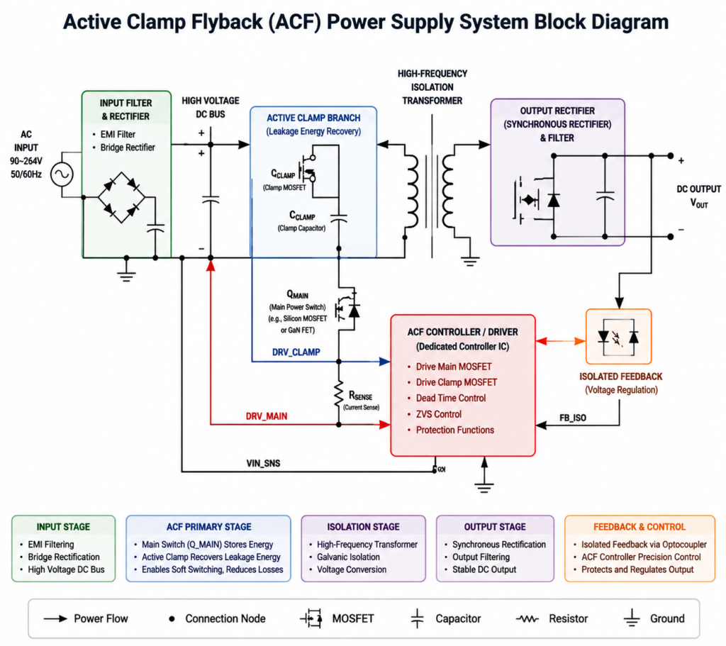
A complete ACF charger circuit consists of six main blocks:
- Input front-end: EMI filter, rectifier bridge, and high-voltage bulk capacitor — convert AC line voltage into a smooth DC bus.
- Main power switch: The “main gate” of the circuit, controlling the energy storage and release cycle of the transformer; typically a MOSFET or GaN transistor.
- High-frequency isolation transformer: The “energy transfer hub”, which performs voltage conversion and provides input-output galvanic isolation.
- Active clamp branch: The core of ACF, made of a clamp switch and clamp capacitor — absorbs leakage energy, limits voltage spikes, and recycles energy.
- Dedicated controller: The “command center”, precisely controlling the on/off sequence and dead time of both switches to ensure reliable ZVS operation.
- Output stage: Synchronous rectifier, output filter capacitor, and PD protocol controller — convert the high-frequency transformer output into stable low-voltage DC.
3. How ACF Works: A Step-by-Step Breakdown
ACF operation repeats in four continuous stages. Below is a plain-language explanation accessible to readers without an electronics background.
3.1 Stage 1: Main Switch On — Transformer Stores Energy
The main switch turns on, applying the DC bus voltage across the transformer primary winding. Current ramps up, and electrical energy is stored in the transformer core as a magnetic field.
During this stage, the secondary-side rectifier is off, and the output capacitor supplies power to the load — similar to a reservoir closing its gate to store water.
3.2 Stage 2: Main Switch Off — Main Energy Flows to the Output
The main switch turns off. The main energy stored in the transformer is released to the secondary side, the secondary rectifier conducts, and power flows to the output load.
However, the energy trapped in the leakage inductance cannot reach the secondary side. Unchecked, it would create a high-voltage spike that damages the main switch. In a conventional flyback, this energy is burned off as heat by the RCD snubber. In ACF, the clamp branch takes over.
3.3 Stage 3: Clamp Branch Activates — Leakage Energy is Captured
Shortly after the main switch turns off, the clamp switch turns on at a precisely timed moment. The energy from the leakage inductance is transferred into the clamp capacitor and temporarily stored. The voltage is clamped to a safe level, and no dangerous spike occurs.
This step is like collecting wastewater into a holding tank instead of pouring it down the drain.
3.4 Stage 4: Resonant Reset — Zero-Voltage Switching (ZVS)
The clamp switch turns off. The leakage inductance resonates with the parasitic capacitance of the main switch, causing the voltage across the main switch to drop. When the voltage falls to nearly 0V, the controller turns the main switch on.
This is Zero-Voltage Switching (ZVS) — opening the gate when the voltage across it is already near zero, so there is almost no surge, and almost no turn-on switching loss.
At this point, one full operating cycle is complete, and the circuit begins the next cycle.
4. Why ACF Achieves Higher Efficiency
Many people know ACF is more efficient, but not exactly why. The efficiency gain comes from multiple mechanisms working together.
4.1 Leakage Energy Recycling: Turning Waste Heat Into Usable Power
In a conventional flyback, 100% of the leakage inductance energy is wasted as heat through the snubber resistor — and the higher the power and frequency, the worse the waste.
ACF recovers this energy via the clamp branch and feeds it back into the circuit for the next cycle. This improvement alone can boost efficiency by around 2% while significantly reducing heat generation.
4.2 Soft Switching: Dramatically Lower Switching Losses
Switch losses come from two sources: conduction loss from the on-resistance, and switching loss from voltage-current overlap during transitions. The latter dominates at high frequencies.
ZVS turn-on eliminates almost all turn-on loss. At high switching frequencies, this gain is even more significant than leakage energy recovery.
4.3 Lower Voltage Stress: Better Device Selection and Lower Conduction Loss
Conventional flyback requires high-voltage-rated switches to survive the large spikes. Higher-voltage parts generally have higher on-resistance, which increases conduction loss.
With ACF clamping the voltage tightly, switches can be selected with lower voltage ratings and lower on-resistance, further reducing conduction losses.
4.4 Higher Frequency Operation: Smaller Size Without Efficiency Penalty
In conventional flyback, increasing frequency causes losses to skyrocket, defeating the purpose.
Because ACF solves the switching loss problem, it can operate at 200 kHz to 1 MHz or more — up from the typical 65 kHz of traditional designs. Higher frequency means smaller transformers and capacitors, which is the main reason chargers keep getting smaller.
5. Full Comparison: ACF vs. Conventional RCD Flyback
The table below summarizes the differences across seven key dimensions:
| Parameter | Conventional RCD Flyback | Active Clamp Flyback (ACF) |
|---|---|---|
| Leakage energy handling | Dissipated as heat | Actively recovered and reused |
| Switching mode | Hard switching | Zero-Voltage Switching (ZVS) |
| Switch voltage stress | High spikes; requires high-voltage parts | Well-clamped; lower stress |
| Typical efficiency gain | Baseline | 3%–5% improvement across load range |
| Circuit complexity | Simple; single-switch control | More complex; dual-switch timing |
| Bill-of-materials cost | Low | Higher; requires dedicated controller IC |
| Design difficulty | Low; mature solutions | Higher; requires careful tuning |
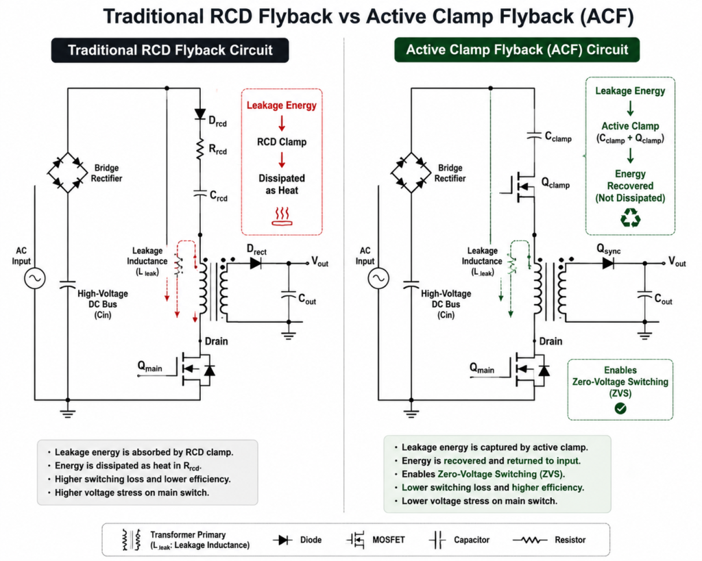
Neither topology is universally better. Conventional flyback excels at low cost and mature design, and is ideal for cost-sensitive applications where size is not critical. ACF excels at performance, and targets mid-to-high-end compact and efficient products.
6. Key Advantages of Active Clamp Flyback
6.1 Superior Efficiency Meets Global Energy Standards
ACF improves full-load efficiency by 3%–5% and reduces no-load power consumption.
It easily meets international energy regulations such as U.S. DoE Level VI and EU CoC Tier 2 — a major reason why global brands are rapidly adopting ACF.
6.2 High Power Density Enables Compact Chargers
Thanks to its high-frequency capability, ACF designs can reduce transformer and filter component size by more than 50%.
When paired with GaN devices, power density can effectively double, making it the core technology behind today’s ultra-compact fast chargers and portable adapters.
6.3 Improved Reliability and Better Thermal Management
Voltage stress on the main switch is reduced by over 30%, eliminating the destructive impact of voltage spikes.
At the same time, lower overall losses mean lower operating temperatures, more stable long-term performance, and longer product life.
6.4 Reduced EMI Emissions
Conventional hard switching produces very steep voltage edges and strong electromagnetic noise, requiring complex filter networks to pass compliance.
ACF produces much smoother switching waveforms with greatly reduced dv/dt and di/dt. This not only lowers EMI, but also allows simpler filter circuits, saving space and cost.
6.5 Wide Input Voltage Capability
ACF maintains high efficiency across the full 85–265Vac global line voltage range, and delivers stable performance from no-load to full-load — ideal for consumer electronics sold worldwide.
7. Limitations and Challenges of ACF
For all its benefits, ACF is not a perfect solution and has inherent tradeoffs.
7.1 Higher Complexity and Strict Timing Requirements
While conventional flyback controls only one switch, ACF must control two switches simultaneously — and with very precise timing and dead time.
Too little dead time can cause shoot-through (both switches on at once), shorting and destroying components. Too much dead time loses the ZVS condition and reduces efficiency. This places strict demands on the controller IC.
7.2 Higher Material Cost
Compared to conventional flyback, ACF requires an additional clamp switch and a dedicated ACF controller IC, such as the UCC28780 from Texas Instruments (U.S.) or the TEA1906 from NXP (Netherlands).
More components and specialized silicon mean a higher bill-of-materials cost.
7.3 ZVS Can Degrade at Light Load
Achieving ZVS requires enough magnetizing energy to drive the resonant cycle.
At light loads, the transformer stores less energy, and there may not be enough to sustain resonant ZVS, causing light-load efficiency to drop. Premium designs add special control techniques to optimize light-load efficiency and standby power.
7.4 Steeper Design and Debugging Learning Curve
ACF performance is highly dependent on parameter matching: transformer leakage inductance, clamp capacitor value, and switching timing must all be precisely tuned. Even small deviations can lead to sub-par efficiency.
As a result, development and debugging take longer than conventional flyback, and require more experienced design engineers.
8. Key Technical Considerations for ACF Implementation
A well-optimized ACF design relies on several critical technical choices.
8.1 Dead Time Control
Dead time — the interval when both switches are off — is the key parameter that ensures ZVS and prevents shoot-through.
Modern high-end ACF controllers include adaptive dead-time regulation, automatically adjusting dead time across load conditions to maintain optimal performance.
8.2 Resonant Component Tuning
Leakage inductance and clamp capacitance together determine the resonant frequency and the ZVS timing window.
Incorrect values directly degrade soft-switching performance and overall efficiency. Proper calculation and lab tuning are required for the target power level and switching frequency.
8.3 Power Device Selection
ACF works with several types of power devices:
- Silicon MOSFETs: Low-cost option for medium-frequency ACF designs, offering good value.
- GaN transistors: Excellent high-frequency performance and fast switching. When combined with ACF, they maximize the benefits of high-frequency miniaturization, and are the mainstream choice for premium fast chargers.
8.4 Pairing With Synchronous Rectification
ACF optimizes losses on the primary input side, while synchronous rectification optimizes losses on the output side.
Primary-side ACF + secondary-side synchronous rectification is today’s standard combination for high-efficiency chargers, delivering efficiency gains across the entire power train.
9. Common Applications and Power Range
9.1 Consumer Fast Charging
This is the largest application for ACF today: GaN fast chargers for phones and tablets, and compact USB-C power adapters for laptops.
For products where portability matters, ACF has become nearly standard.
9.2 Home Appliance and Industrial Auxiliary Power
Standby power supplies for TVs, air conditioners, and low-power auxiliary modules in industrial equipment are also increasingly using ACF.
The main drivers are tighter energy regulations, lower standby power, and improved long-term reliability.
9.3 IoT and Smart Home Power Supplies
Routers, set-top boxes, and low-power smart device adapters are gradually adopting ACF, primarily to reduce standby power and improve overall energy efficiency.
9.4 Optimal Power Range
ACF is most commonly used in the 20 W to 200 W low-to-medium power range.
Within this range, it offers the best balance of isolation, efficiency, size, and cost. At higher power levels, LLC resonant topologies generally become more advantageous.
10. Common Misconceptions Clarified
10.1 Myth: ACF only works with GaN transistors
This is the most common misconception. In reality, ACF works perfectly well with silicon MOSFETs — many early high-efficiency adapters used silicon-based ACF designs.
GaN and ACF are complementary: GaN amplifies the high-frequency benefits of ACF, but it is not a requirement.
10.2 Myth: ACF wasn’t used in old chargers because it hadn’t been invented yet
The principles of ACF have been known for decades — it is not a new technology.
It was not widely adopted in the past because dedicated controller ICs were very expensive, and global energy efficiency standards were more lenient. Only in recent years, as regulations tightened and IC costs fell, has ACF become mainstream in consumer electronics.
10.3 Myth: ACF is always more efficient than LLC resonant topology
This is incorrect. The two topologies excel at different power levels.
Above roughly 200 W, LLC resonant topologies typically deliver higher efficiency and better overall performance. Below 200 W, ACF offers a simpler structure and better cost-performance balance.
11. Future Technology Trends
11.1 Deeper Integration With Wide-Bandgap Devices
ACF will continue to evolve alongside GaN and silicon carbide (SiC) wide-bandgap devices, moving toward even higher frequencies and higher power density for even smaller chargers.
11.2 Highly Integrated Controller ICs
ACF controllers will become more integrated, incorporating drivers, sensing, and protection features on-chip to reduce external component count.
This will not only shrink solution size, but also lower design barriers and help ACF spread into lower-power applications.
11.3 Support for Higher-Power Fast Charging Standards
With the rollout of higher-power standards like USB PD 3.1 EPR at 140 W and 240 W, ACF will expand into higher-power adapter designs.
11.4 Digital Control and Smart Optimization
More designs will adopt digital controllers with adaptive algorithms that dynamically adjust timing and frequency, optimizing both heavy-load efficiency and light-load standby performance across all operating conditions.
12. Conclusion
Active Clamp Flyback is a milestone upgrade to the conventional flyback topology. Instead of reinventing the flyback, it delivers two key improvements — active clamp for leakage energy recovery, and zero-voltage soft switching — trading a modest increase in cost and complexity for major gains in efficiency, power density, and reliability.
For most consumers, you don’t need to remember the term ACF. You will simply see its benefits in the charger you hold: smaller size, lower heat, and better energy efficiency. It is today’s leading advanced topology for low-to-medium power isolated supplies, balancing performance and cost, and forming the technical foundation of the modern compact fast charger.
FAQ
Q: What is the relationship between Active Clamp Flyback and regular flyback?
A: ACF is an upgraded and improved version of the conventional flyback topology. The core transformer energy storage and release logic remains the same; the main changes are in how leakage energy is handled and how the switches operate.
Q: Do regular shoppers need to look for “ACF” when buying a charger?
A: No, you don’t need to seek out this technical spec. ACF is an internal circuit technology whose benefits show up as smaller size, lower heat, and better efficiency — just evaluate the charger’s actual size, power rating, and thermal performance.
Q: Will ACF completely replace conventional flyback?
A: No. Conventional flyback still holds a strong cost advantage in low-end, cost-sensitive applications where size and efficiency are less critical. ACF targets the mid-to-high-end compact and efficient charger market.
Q: How many types of Active Clamp Flyback structures are there?
A: Based on the position of the clamp switch, there are high-side clamp and low-side clamp configurations. High-side NMOS clamp is the dominant approach used in consumer electronics chargers today.