
Quick Summary
- Core definition: Synchronous rectification (SR) replaces traditional diodes with controlled MOSFET electronic switches to perform rectification — an upgrade from passive conduction to active, controllable power conversion.
- Key benefit: In low-voltage, high-current applications like phone and laptop fast chargers, SR cuts rectification losses and boosts efficiency by 5% to 15%, significantly reducing heat buildup.
- Where you’ll find it: USB-C PD chargers, GaN wall adapters, laptop power bricks, and other high-power-density consumer electronics.
- Technical role: One of the foundational technologies that enable modern high-performance chargers to run efficiently in a compact form factor.
1. The Hidden Problem: Why Traditional Rectification Hits a Wall
1.1 How Diode Rectification Works
Before we dive into synchronous rectification, let’s cover the basics of what rectification does.
Your wall outlet delivers alternating current (AC), but your phone and laptop run on direct current (DC). Rectification is the step that converts bidirectional AC into unidirectional DC — it’s like sorting traffic to all flow in one direction.
For decades, diodes handled this job. A diode is a passive component with a simple physical rule: current flows easily in one direction, and is blocked in the reverse direction, like a one-way gate in a circuit. Chargers typically use Schottky diodes, which have lower forward voltage drop than standard silicon diodes.
1.2 The Unavoidable Physical Tradeoff
Diodes are simple and reliable, but they have a built-in flaw you can’t engineer around: current always loses a small amount of voltage when passing through, called the forward voltage drop. It’s like a small step at the bottom of the one-way gate — every electron that passes loses a little energy.
- Standard silicon diodes have a forward drop of roughly 0.6–0.7V
- Schottky diodes have a lower forward drop of roughly 0.3–0.5V
The power lost to this drop follows a straightforward formula: Power loss = Forward voltage × Output current (P = Vf × I).
Loss grows linearly with current. To put this in perspective:
- At 5V/3A (a common phone fast-charging level), a 0.4V drop in a Schottky diode wastes 1.2W — about 8% of the total output power.
- At 20V/5A (100W laptop charging), that same 0.4V drop wastes 2W, and heat becomes a much bigger problem.
The lower the output voltage and the higher the current, the bigger share of total power this fixed drop consumes. That’s the hard physical limit of diode rectification.
1.3 How Synchronous Rectification Solves It
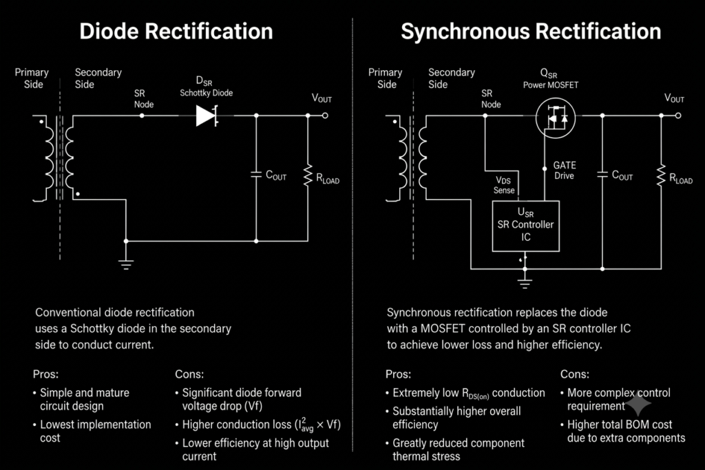
Synchronous rectification breaks through this limit by replacing the diode with a different kind of component: a power MOSFET.
A MOSFET is essentially a very fast, controllable electronic switch. When turned on, it conducts through an extremely low on-resistance (Rds(on)) — often just a few milliohms in high-quality parts. Its loss formula is different: Power loss = Current² × On-resistance (P = I² × R).
At high currents, the voltage drop across a milliohm-scale resistor is far smaller than the fixed drop of a diode, so losses plummet.
To make a MOSFET act like a one-way rectifier, a control circuit precisely times when it turns on and off: on when current flows forward, off before current can reverse.
This combination of active switch control and ultra-low conduction loss is synchronous rectification. It represents a shift from passive, unguided rectification to active, managed rectification — all to deliver higher efficiency, less heat, and more power in less space.
1.4 A Simple Real-World Analogy
Think of the two rectification methods like doors on a building:
- Diode rectification: A heavy one-way swing door with a raised threshold. You can only push through one way, and everyone loses a little energy stepping over the threshold.
- Synchronous rectification: An automatic sliding door with motion sensors. It slides open smoothly when someone approaches from the right direction, has almost no threshold to step over, and stays closed if someone approaches from the wrong side.
2. How It Works Inside a Typical Flyback Charger
Nearly all phone chargers and mid-power fast adapters use a flyback power topology. We’ll use this most common design to explain how synchronous rectification operates in real products.
2.1 The Two-Stage Rhythm of a Flyback Converter
At the heart of a flyback charger is a high-frequency transformer that works in two repeating phases:
- Primary conduction phase: The main switch on the input side turns on, current flows through the primary winding, and the transformer stores energy in its magnetic field. No current flows on the secondary (output) side during this phase.
- Secondary freewheeling phase: The primary switch turns off, the transformer releases its stored energy, and current flows out of the secondary winding to power your device. The rectifier on the secondary side conducts during this phase.
In a traditional design, that secondary rectifier is a Schottky diode. In a synchronous rectification design, that diode is replaced with a power MOSFET.
2.2 Replacement Logic and Precise Timing
Swapping the part is easy. The real engineering is in the “synchronous” part: the MOSFET’s on/off timing must perfectly match the transformer’s rhythm and the direction of current on the secondary side.
- When the primary switch turns off and the secondary winding voltage goes positive, the control circuit turns the MOSFET on immediately, letting current flow with very little resistance.
- When the transformer’s stored energy is nearly exhausted and secondary current is about to reverse, the control circuit turns the MOSFET off early to prevent current from flowing backward into the transformer.
The word “synchronous” refers to this precise alignment with the main switch timing and current direction — it does not mean synchronized with your wall outlet’s AC frequency.
2.3 Dead Time: The Critical Safety Buffer
There is a short safety window built into every switching transition called dead time.
If the primary main switch and the secondary synchronous rectifier were ever on at the same time, it would short-circuit the transformer and destroy parts instantly. So between “primary off → secondary on” and “secondary off → primary on”, there is a brief gap where both switches are off. That gap is dead time.
Too much dead time means the MOSFET’s built-in body diode conducts longer, increasing losses. Too little dead time risks a shoot-through short. Modern SR controllers use adaptive dead-time adjustment to dynamically tune this window for the best balance of safety and efficiency.
2.4 Waveforms and the Built-In Backup
On an electrical level, the MOSFET’s drive signal lines up exactly with its drain-source voltage: when the voltage drops to the body diode’s conduction threshold, the drive signal turns the MOSFET on; when current nears zero, the drive signal turns it off early.
During dead time, the MOSFET itself is off, but current still flows temporarily through its internal body diode — essentially a built-in backup diode that keeps the circuit running. This fallback is a basic but important reliability feature of every synchronous rectifier.
3. Control Logic and Key Technical Details
Synchronous rectification isn’t just about swapping a part. Its real performance depends on the precision of its control logic.
3.1 How the Controller Knows When to Switch
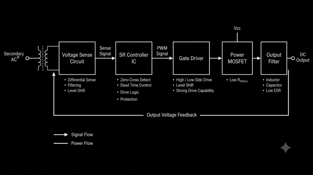
How does the control chip decide exactly when to turn the MOSFET on and off? Two main methods are used:
- Vds voltage sensing: The chip monitors the voltage across the MOSFET to detect when its body diode starts conducting, which indicates forward current flow. This is the dominant approach in consumer chargers — low cost and simple to implement.
- Current sensing: A small sense resistor directly measures current direction for higher accuracy. This costs more and adds complexity, so it’s mostly found in industrial and high-end power supplies.
3.2 The Evolution of Dead-Time Tuning
Early SR designs used fixed dead time, optimized for only one specific load level. Efficiency suffered at lighter and heavier loads.
Nearly all modern controllers now use adaptive dead-time adjustment. They dynamically tweak the timing based on real-time load current and input voltage, minimizing body-diode conduction while staying safely above the shoot-through risk. This delivers better efficiency across the entire load range.
3.3 Solving the Light-Load Efficiency Problem
Synchronous rectification shines at high current, but it runs into a drawback at light loads.
When output current is very low, the power consumed by the MOSFET’s drive circuit can eat into — or even outweigh — the energy saved by lower conduction loss. Under those conditions, a plain diode can actually be more efficient. Poor timing can also cause current to flow backward.
The industry’s main solutions are diode emulation mode and burst mode. At light loads, the MOSFET either mimics diode behavior or switches on and off intermittently to cut drive losses, balancing efficiency across both heavy and light use.
3.4 Advanced Challenge: Reverse Recovery in CCM
In high-power continuous conduction mode (CCM), there’s another subtle issue: the MOSFET’s body diode has a small reverse recovery time (trr) when turning off. This causes voltage ringing, extra losses, and higher electromagnetic interference.
Designers address this in two main ways: choosing MOSFETs with better reverse recovery characteristics, and adding RC snubber circuits to dampen ringing and suppress noise.
4. Side-by-Side: Synchronous Rectification vs. Diode Rectification
The table below compares the two approaches across the factors that matter most for real-world chargers.
| Comparison Category | Traditional Diode Rectification | Synchronous Rectification |
|---|---|---|
| Core nature | Passive component; relies on physical properties for one-way conduction | Active system; uses a controller chip to actively switch on and off |
| Loss behavior | Fixed forward voltage drop; loss scales linearly with current | Ultra-low on-resistance; loss scales with the square of current |
| High-current efficiency | Low; fixed drop becomes a large share of total loss | Very high; conduction loss is far lower than a diode |
| Light-load efficiency | Stable; no extra drive overhead | Moderate; drive losses reduce the net benefit |
| Heat output | High heat from the rectifier stage | Significantly reduced heat from rectification |
| Bill of materials cost | Low; a single diode does the job | Higher; requires a MOSFET plus a dedicated controller |
| Design complexity | Very low; simple circuit with minimal tuning | Higher; requires timing control, careful PCB layout, and EMI filtering |
| Best suited for | Low-power, high-voltage, cost-sensitive products | Low-voltage/high-current, high-power-density, high-performance fast chargers |
4.1 Where Each Technology Makes Sense
The two approaches have clear, well-understood use cases:
- Choose synchronous rectification for low-voltage (≤12V), high-current (≥5A) designs such as phone fast chargers and laptop adapters — and any product where small size and low heat are priorities, like GaN chargers.
- Choose diode rectification for high-voltage, low-power (<15W), or extremely cost-sensitive products, such as basic 5W phone chargers and small appliance power supplies.
- Hybrid approach: Some mid-range designs use both — running in diode mode at light load and switching to full synchronous rectification at heavy load — to balance efficiency and cost across all conditions.
5. How SR Is Implemented in Common Charger Topologies
Synchronous rectification takes different forms depending on the power topology, and matches different charger power levels.
5.1 Quasi-Resonant Flyback (QR Flyback)
Quasi-resonant flyback is the dominant topology for 65W–100W consumer fast chargers, and where synchronous rectification is most widely adopted.
These designs use single-switch secondary-side synchronous rectification, directly replacing the Schottky diode. The technology is mature, cost-effective, and offers the best balance of price and performance. Most 65W GaN chargers on the market use this exact QR flyback + single SR architecture.
5.2 LLC Resonant Converter
The LLC resonant topology is the standard for 100W+ high-power GaN chargers, where maximum efficiency is the goal.
LLC designs typically use center-tapped dual-switch synchronous rectification on the secondary side. Two SR MOSFETs alternate conduction, and when paired with primary-side zero-voltage switching (ZVS), they push overall efficiency above 95% with exceptionally low heat. Today’s 120W, 140W, and even 240W high-end chargers almost universally use LLC + dual SR.
5.3 Buck Converters
Beyond the main AC-DC stage, synchronous rectification also appears in secondary DC-DC stages inside chargers — such as step-down converters and cable drop compensation circuits. Here it’s usually called synchronous freewheeling.
A synchronous buck converter uses a high-side main switch and a low-side synchronous freewheeling MOSFET, replacing the traditional freewheeling diode. This cuts losses in the step-down stage and raises overall system efficiency.
5.4 Design Challenge: Driving MOSFETs at Very Low Output Voltages
A MOSFET needs roughly 10V of gate drive to turn on reliably. But in low-output designs — for example 3.3V or 5V outputs — the output voltage alone isn’t enough to drive the gate.
Engineers solve this with auxiliary transformer windings, bootstrap supply circuits, or MOSFETs rated for lower gate voltages, ensuring synchronous rectification works properly even at very low output levels.
6. Why Fast Chargers Need Synchronous Rectification
Synchronous rectification moved from industrial power supplies into every consumer’s wall adapter for several converging reasons.
6.1 Ever-Rising Fast-Charging Power Levels
Fast-charging power has grown dramatically over the years: from 5W basic charging, to 18W and 25W mainstream fast charge, to today’s 65W and 100W standards — and even 240W USB PD EPR for the highest-performance laptops.
More power means more current, and diode losses scale directly with current. At 20V/5A, the heat from a traditional Schottky rectifier becomes unacceptable. Synchronous rectification is the only practical way to bring rectification losses down and make high-power charging viable.
6.2 The Push for Higher Power Density
Gallium nitride (GaN) power devices have let designers raise switching frequencies dramatically, shrinking transformers and capacitors and making chargers much more compact.
But smaller cases mean far less space for heat dissipation. Heat sinks alone can’t solve the problem. Synchronous rectification cuts conduction losses at the source, reducing total heat generation. It’s an essential technology for making small, high-power GaN chargers work reliably.
6.3 Global Energy Efficiency Regulations
Major markets around the world enforce strict efficiency rules for power adapters, pushing manufacturers to raise conversion performance:
- The U.S. Department of Energy (DoE) Level VI standard sets mandatory average efficiency and no-load power limits.
- The European Union’s CoC Tier 2 Code of Conduct sets even tighter efficiency requirements.
Traditional diode rectifiers struggle to meet these higher tiers. Synchronous rectification has become a standard technique to pass certification.
6.4 A Better User Experience
For end users, the benefits are tangible:
- Charger case temperatures stay lower, even during long, high-power charging sessions.
- Higher efficiency means less wasted electricity over time.
- Cooler-running components also tend to have longer service lives.
7. It Takes a System: SR Works Alongside Other Key Technologies
Synchronous rectification isn’t a standalone feature. It’s one piece of a modern high-efficiency power system, working with other technologies to deliver top-tier performance.
7.1 The Three Pillars of a High-Efficiency Adapter
A high-performance GaN fast charger rests on three core technologies:
- Power Factor Correction (PFC): Improves grid-side power utilization, reduces reactive losses, and meets harmonic standards.
- GaN power devices: Raise primary-side switching frequency, drastically shrinking transformers and passives for a smaller product.
- Synchronous rectification (SR): Eliminates the secondary-side conduction loss bottleneck, boosting overall efficiency and controlling heat.
Each handles a different part of the problem, and together they create a charger that’s small, efficient, and cool-running.
7.2 The Gold Standard: LLC + SR
In high-power chargers, LLC resonant topology plus synchronous rectification is the gold-standard combination:
- LLC enables zero-voltage switching (ZVS) on the primary side, nearly eliminating switching losses.
- Synchronous rectification slashes conduction losses on the secondary side.
Tackling both switching loss and conduction loss pushes total efficiency above 95%, and is the default architecture in premium high-power adapters.
7.3 The Shift Toward Digital Control
Traditional SR controllers are analog chips — fast and low-cost, but with fixed parameters optimized for one operating point.
Digital control is now making its way into consumer products. An MCU or DSP manages SR timing, adapts automatically across the full load range, and can coordinate with other charger functions. It’s more flexible and achieves higher peak efficiency, and will become the norm in premium chargers over time.
8. Limitations and Design Tradeoffs
For all its benefits, synchronous rectification is not a universal solution, and it comes with real tradeoffs and challenges.
8.1 Where It’s Irreplaceable
In low-voltage, high-current, high-power-density designs, synchronous rectification has no equal. As long as charging power keeps rising and chargers keep shrinking, SR will remain indispensable.
8.2 Inherent Limits and Industry Solutions
- Higher complexity: Compared to a single diode, SR adds a controller chip, drive circuitry, and stricter requirements for PCB layout and EMI filtering. The industry addresses this with highly integrated controller chips and proven reference designs that reduce engineering effort.
- Light-load efficiency gap: Drive losses reduce the benefit at low current. Modern controllers solve this with burst mode and diode emulation, balancing light-load and heavy-load performance.
- Poor value at very low power: Below 15W, the efficiency gain from SR is small but the cost adder is meaningful. That’s why basic low-power chargers still rely on diodes.
8.3 Reliability and Protection
A common question is: what happens if the SR controller fails? Will the charger short out?
Reputable SR controller chips include full protection features: over-voltage, over-current, and over-temperature protection. Even if the control circuit fails, the MOSFET’s body diode can still act as a basic rectifier — it won’t cause a direct short. Combined with fuses and other safety layers in a well-designed charger, the overall system is very reliable.
9. Common Myths and FAQs
9.1 Common Misconceptions
Myth 1: Synchronous rectification is always more efficient than a diode, at any load.
Reality: No. SR excels at medium and heavy loads. At very light loads, drive power can outweigh the conduction savings, and a simple diode can be slightly more efficient. Good SR designs include light-load optimizations to narrow this gap, but they can’t eliminate it entirely.
Myth 2: All GaN chargers use synchronous rectification.
Reality: The two are separate technologies. GaN is the primary-side switch; SR is the secondary-side rectifier. Some budget GaN chargers skip SR to cut costs and keep using a Schottky diode. Those models generally run hotter.
Myth 3: The lower the MOSFET on-resistance, the better the SR performance.
Reality: On-resistance isn’t the only factor. SR MOSFETs require a balance of on-resistance, gate charge, and parasitic capacitance. A part with extremely low resistance often has higher gate charge, which increases drive losses and can hurt performance at high frequencies.
Myth 4: A charger with SR won’t get warm at all.
Reality: It runs cooler, not cold. Energy conversion always produces some loss, and transformers, switches, and capacitors all generate heat. SR only addresses rectification losses — it doesn’t eliminate all heat from the charger.
9.2 FAQs for General Readers
Q: Why don’t 5W and 10W chargers use SR?
It mostly comes down to cost vs. benefit. At low power and low current, diode losses are already small. SR saves very little energy but adds noticeable cost and complexity, so the tradeoff isn’t worth it.
Q: How can I tell if a charger has synchronous rectification?
You can’t tell from the outside. The most reliable way is to look at professional teardown reviews, which show whether there’s an SR controller IC and matching MOSFET on the secondary side. As a general rule, reputable 65W+ fast chargers and GaN adapters almost always include SR.
Q: Does synchronous rectification make chargers more expensive?
It adds a small amount to the bill of materials, but as the technology has matured, that premium has shrunk. For most users, the real-world benefits — lower temperature and higher efficiency — are well worth the modest cost increase.
9.3 Advanced Technical FAQs
Q: Is EMI harder to manage with SR than with diodes?
Yes. MOSFETs switch much faster, creating steeper voltage and current transitions that generate more electromagnetic interference. SR designs require more careful PCB layout, snubber circuits, and filtering to meet EMI standards — that’s part of why they’re harder to design.
Q: Can you test for SR without taking the charger apart?
You can infer it from an efficiency curve: a pure diode charger sees efficiency drop steadily as current rises, while an SR design peaks in the mid-load range and dips slightly at both very light and very heavy loads. The most definitive answer, though, still comes from a teardown.
10. Summary and Future Outlook
10.1 Why This Technology Matters
Synchronous rectification is a fundamental advance in power electronics. By replacing passive diodes with actively controlled low-resistance switches, it breaks through the long-standing efficiency limit of traditional rectification.
For consumer electronics, it’s the efficiency foundation that makes modern high-power-density adapters possible. It enables faster charging in smaller cases, and it aligns with global goals for lower energy waste and reduced carbon emissions.
10.2 Where the Technology Is Headed
Several trends will shape the next generation of synchronous rectification:
- Wider adoption of digital adaptive control: Digital SR will move from industrial use into mainstream consumer products, delivering smarter optimization across every load level.
- Highly integrated combo chips: Packaging the SR controller and power MOSFET into a single package reduces external parts, simplifies design, and saves board space.
- Wide-bandgap semiconductors: Silicon carbide (SiC) and other third-generation semiconductors will expand into high-voltage SR applications, raising the performance ceiling even further.
- Higher switching frequencies: Paired with GaN and other advanced devices, SR will keep pushing to higher frequencies for even greater power density.
10.3 What It Means for You
For everyday users, the steady advance of synchronous rectification shows up as simple, tangible improvements: chargers that are smaller and lighter, cooler to the touch during a long charge, faster at topping up your devices, and a little more efficient with every watt.
It’s the kind of invisible technology that makes your daily experience better — one small engineering improvement at a time.