
Quick Summary: What You’ll Learn in 3 Minutes
If you’ve ever wondered why some chargers feel “cleaner” than others, or why your audio gear picks up mysterious hum, this guide is for you. Ripple and noise testing is the gold standard for judging power supply quality — and it matters far more than most people realize.
Key takeaways upfront:
- Ripple is the periodic voltage fluctuation found on DC power outputs, most commonly from switching supplies
- Noise includes both random broadband interference and sharp switching transients
- The 20 MHz bandwidth limit is a widely adopted industry convention for standardized ripple readings
- A properly executed test depends more on probe technique than expensive lab equipment
- USB-C PD, PPS, and EPR modes each present unique testing challenges for modern chargers
Whether you’re a tech reviewer, hobbyist engineer, product buyer, or just someone who wants to understand what makes a good charger — this guide walks you through everything from basic concepts to hands-on measurement procedures.
1. Fundamentals: What Are Ripple and Noise?
1.1 What Is Power Supply Ripple?
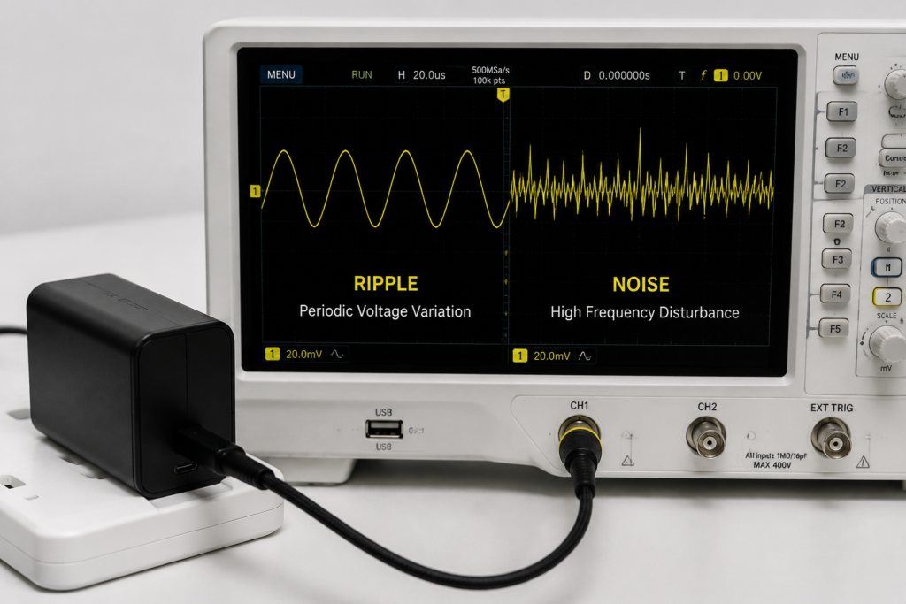
Ripple is the regular, repeating AC voltage component that sits on top of an otherwise steady DC output. Think of it like gentle ocean waves on a calm sea — predictable, cyclical, and tied to the power supply’s internal rhythm.
Ripple is not exclusive to switching power supplies. Any DC power source can contain periodic voltage variations, but in modern consumer electronics, switching power supplies (SMPS) are by far the most common source.
It comes from two primary origins:
- Line-frequency ripple (100 Hz / 120 Hz): Residual variation left over from the AC rectification stage, typically very low amplitude in modern designs
- Switching-frequency ripple (kHz to MHz range): Generated by the on/off cycling of power transistors and the charging/discharging of inductors and capacitors
Unlike random noise, ripple is predictable. Its frequency matches — or is a multiple of — the power supply’s switching frequency.
1.2 What Is Power Supply Noise?
Noise encompasses all unwanted voltage disturbances that are not part of the regular, low-frequency ripple pattern. It’s the static, crackle, and sharp spikes riding on top of the ripple wave.
Noise typically falls into two broad categories:
- True random noise
- Thermal noise from resistive components
- Shot noise in semiconductor junctions
- Truly random, broadband, and present at all times
- Switching-related high-frequency disturbances
- MOSFET turn-on and turn-off spikes
- Ringing and parasitic oscillation in inductive circuits
- Repetitive and synchronized with the switching clock, but fast and narrow rather than smooth
Noise is further classified by how it travels:
- Conducted noise: Travels along power wires and PCB traces
- Radiated noise: Escapes as electromagnetic fields through the air
- Differential-mode noise: Appears across the positive and negative output lines
- Common-mode noise: Appears identically on both lines relative to ground
Important clarification: Ripple & noise testing measures output voltage quality at the power supply terminals. EMI testing measures electromagnetic radiation and conduction for regulatory compliance. They are related but separate disciplines.
1.3 Ripple vs. Noise: Core Differences
| Aspect | Ripple | Noise |
|---|---|---|
| Signal nature | Periodic, predictable | Mix of random and transient, irregular |
| Primary source | Rectification, switching cycles, LC filtering | Switching transients, parasitics, EMI coupling |
| Frequency range | Line frequency to switching harmonics | Broadband, often extending into tens of MHz |
| Waveform shape | Smooth sinusoidal or triangular | Sharp spikes, hash, fuzzy bands |
| Optimization approach | Larger capacitors, better filtering | Shielding, layout, snubbers, slower edges |
In real-world measurements, you see both at once — ripple forms the baseline wave, and noise rides on top of it as fine “hair” or sharp spikes.
1.4 Ripple, Voltage Regulation, and Load Transient: Key Distinctions
These three terms are often confused, but they describe completely different things:
| Metric | What it measures | Time scale | Test tool |
|---|---|---|---|
| Ripple & Noise | High-frequency AC variation on the DC rail | Microseconds to nanoseconds | Oscilloscope |
| Voltage regulation | How well output voltage stays at its nominal value under steady load | Seconds to minutes | Multimeter, power analyzer |
| Load transient response | How much voltage dips/spikes and recovers when load current changes | Milliseconds to microseconds | Oscilloscope, dynamic load |
In short: ripple is a steady-state high-frequency wobble; regulation is DC accuracy; transient response is how the supply recovers from a sudden load change. Many casual reviews mistakenly count transient voltage dips as “ripple.”
1.5 Why Ripple and Noise Matter for Everyday Devices
You might not see ripple on your screen, but your electronics feel it every day.
For smartphones and fast charging:
- Excessive ripple can interfere with charging protocol communication
- Poor power quality can cause erratic charging speeds or protocol drops
- Long-term stress on battery management circuits may accelerate aging
For laptops and high-power devices:
- Unstable supply rails can cause system instability or unexpected shutdowns
- High-frequency noise can interfere with touchpads, audio, and radio performance
For precision electronics:
- Audio gear develops audible hum and hiss
- Sensors and measurement equipment produce inaccurate readings
- High-speed digital circuits suffer from data errors and glitches
Myth busting: Normal levels of ripple won’t “fry” your phone. Extreme cases with poor design and missing protections can cause instability, but typical consumer chargers — even budget ones — operate within safe voltage ranges. The real difference is in subtle performance and long-term reliability.
2. Where Do Ripple and Noise Come From?
2.1 Inside a Switching Power Supply: The Birthplace of Ripple
Nearly every USB-C charger, laptop adapter, and PC power supply uses switch-mode power supply (SMPS) technology. It works by:
- Rectifying wall AC into high-voltage DC
- Chopping that DC at high frequency (typically 50 kHz – 2 MHz) using power transistors
- Stepping the voltage down through a high-frequency transformer
- Rectifying and filtering the output back to clean DC
The ripple forms at step 4. Even with output capacitors, the voltage dips slightly during each switching cycle when the inductor is releasing energy, then climbs back up when charging. The result is a tiny sawtooth or triangular wave — your ripple voltage.
2.2 Three Core Sources of Noise
1. High-speed switching transients
Every time a MOSFET turns on or off, the voltage and current swing dramatically in mere nanoseconds. These fast edges — described as high dv/dt (how quickly voltage changes over time) and high di/dt (how quickly current changes) — generate sharp noise spikes that couple throughout the circuit.
2. PCB layout and parasitic effects
Every copper trace has tiny amounts of inductance and capacitance. At high switching speeds, these “parasitic” elements become significant. Small loop areas act like antennas, radiating and picking up noise.
3. External electromagnetic coupling
Nearby radios, motors, cell signals, and even other power supplies can inject noise through the air or along power lines. A well-shielded design keeps most of this out.
2.3 GaN Fast Chargers: Why Miniaturization Raises Design Challenges
Gallium Nitride (GaN) transistors have revolutionized charger design — they’re smaller, cooler, and more efficient than traditional silicon MOSFETs. But they also present new noise control challenges.
The advantages:
- Much faster switching = lower switching losses = higher efficiency
- Can run at higher frequencies = smaller transformers and capacitors = tinier chargers
The design challenges:
- Faster voltage edges (higher dv/dt) excite parasitic inductances more strongly
- Higher operating frequencies push noise energy into bands that are harder to filter
- Compact layouts leave less room for shielding and large filter components
This doesn’t mean GaN chargers are inherently noisier — a well-designed GaN charger can outperform a mediocre silicon one. It means engineers have to work harder to keep noise under control when shrinking the form factor.
2.4 Key Design Factors That Shape Ripple and Noise
Several design decisions determine how “clean” a power supply will be:
- Output capacitor selection: Low ESR (Equivalent Series Resistance) and low ESL (Equivalent Series Inductance) capacitors reduce ripple dramatically
- Filter topology: Simple single-capacitor output vs. multi-stage LC or π filters
- Switching frequency: Higher frequencies allow smaller components but can increase noise challenges
- PCB layout: Tight, short high-current loops are the #1 rule for low noise
- Transformer design: Shielded windings reduce common-mode noise coupling
2.5 Testing Traits by Power Supply Type
USB-C PD Chargers
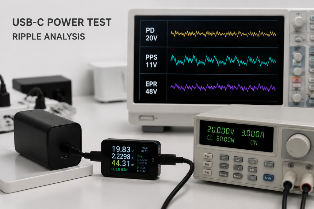
- Must be tested across multiple fixed PDO voltages (5V, 9V, 15V, 20V) and PPS dynamic ranges
- EPR (Extended Power Range) models up to 240W add 28V, 36V, and 48V rails
- Higher power levels generally require stricter noise control
DC-DC Converter Modules (Buck / Boost)
- Buck converters typically have lower output ripple than isolated flyback designs
- Input voltage range affects ripple performance across operating conditions
LDO Linear Regulators
- Much lower output noise than switching regulators
- Standard low-noise LDOs: 0.5 – 5 mVpp typical
- Ultra-low-noise LDOs for RF and instrumentation can reach sub-100µV noise levels
- Test methodology focuses on ultra-low noise measurement techniques
Battery-Powered Devices
- Inherently low ripple environment
- Ripple appears primarily from internal DC-DC converters, not the battery itself
3. Key Metrics: How to Quantify Ripple and Noise
3.1 Peak-to-Peak Voltage (mVpp): The Common Benchmark
Peak-to-peak (Vpp) measures the total voltage difference between the highest peak and the lowest valley on the waveform.
For example, if a 20V output swings from 19.94V to 20.06V, the ripple is 120 mVpp.
This is the most widely used metric because:
- It shows the full extent of voltage variation
- It’s simple to read directly from an oscilloscope
- Component datasheets and industry specs almost always use Vpp
- It captures worst-case spikes that RMS would average out
3.2 RMS Voltage (mVrms): The Energy Perspective
Root Mean Square (RMS) represents the equivalent DC voltage that would deliver the same power into a resistive load. It’s essentially an average that weights higher voltages more heavily.
RMS is useful for:
- Estimating thermal and power effects of noise
- Audio noise measurements (THD+N)
- Comparing broadband noise levels
For a pure sine wave, Vpp ≈ 2.828 × Vrms. But real-world ripple + noise waveforms aren’t clean sine waves, so this conversion is only approximate and should be used with caution.
3.3 Reference Ranges by Application
Ripple acceptability always depends on output voltage, power level, and use case. A 50 mVpp reading means very different things on a 5V rail vs. a 48V rail.
Typical consumer electronics reference ranges (20 MHz bandwidth):
| Application | Typical Ripple & Noise (mVpp) | Notes |
|---|---|---|
| Ultra-low-noise LDOs | < 0.1 | RF, precision instrumentation |
| Standard low-noise LDOs | 0.5 – 5 | Precision analog, high-end audio |
| High-quality 5V USB charger | 10 – 30 | Well-designed budget to premium models |
| 20V laptop / PD charger | 30 – 80 | Normal range for 65W–140W GaN |
| ATX +12V rail (max spec) | ≤ 120 | Intel ATX 3.0 specification limit |
| ATX +5V / +3.3V (max spec) | ≤ 50 | Intel ATX 3.0 specification limit |
Pro tip: Always note the measurement bandwidth when comparing numbers. A 20 MHz bandwidth reading and a full-bandwidth reading can differ dramatically.
3.4 Frequency-Domain Analysis: Locating Noise With FFT
Time-domain oscilloscope views show what the noise looks like. Frequency-domain analysis shows where it comes from.
What FFT does:
- Fast Fourier Transform converts the time-domain waveform into a frequency spectrum
- Each peak on the spectrum corresponds to a specific frequency component
What you can identify:
- The fundamental switching frequency and its harmonic multiples
- Whether a spike comes from the power supply itself or external interference
- Resonances in filter networks or PCB traces
For example: if you see a strong peak at 65 kHz and smaller peaks at 130 kHz, 195 kHz, and so on, you’re looking at the switching frequency and its harmonics — the noise comes directly from the power supply’s switching action. If you see random peaks at broadcast radio frequencies, it’s environmental pickup.
Time-domain testing answers “how much noise?” Frequency-domain testing answers “what kind of noise and where’s it coming from?” Both are valuable tools in a complete evaluation.
4. Test Equipment: What You Need (and What You Don’t)
4.1 Digital Oscilloscope: The Core Tool
An oscilloscope is non-negotiable for ripple and noise work. A multimeter simply can’t capture fast-changing waveforms.
Minimum requirements for charger testing:
- Bandwidth: At least 20 MHz for basic ripple; 100 MHz recommended for full noise analysis
- Sample rate: 500 MSa/s or higher; 1 GSa/s+ preferred for crisp detail
- AC coupling: Essential for removing DC offset and zooming in on the AC component
- 20 MHz bandwidth limit: Standard feature on most scopes
Capability tiers:
- Entry-level (hobbyist / reviewer): 100 MHz digital storage oscilloscope (DSO) — sufficient for most charger and power supply testing
- Mid-range (serious testing): 200 MHz+ scope with FFT capability and good vertical sensitivity
- Professional lab: 500 MHz+ scope with power analysis software, differential probes, and a dedicated spectrum analyzer
4.2 Probes and Grounding: Where Most Measurements Go Wrong
The probe is where accuracy lives — or dies.
Passive probes (1× / 10×)
- 1× mode: No attenuation, higher sensitivity, but lower bandwidth and more circuit loading
- 10× mode: 10:1 attenuation, wider bandwidth, less circuit loading — the most common choice
- Critical rule: Always match the scope’s channel attenuation setting to the probe
The ground spring — your most important accessory
That long alligator clip on your probe? Don’t use it for ripple measurements. The long ground lead creates a loop antenna that picks up massive amounts of environmental noise, inflating your readings by tens or even hundreds of millivolts.
Instead, use a ground spring (also called a ground barrel or bayonet tip) — a short, rigid metal contact that clips directly onto the probe tip barrel. This creates the smallest possible ground loop.
Differential probes
- Used for floating measurements where neither side is ground-referenced
- Reject common-mode noise extremely well
- Useful for certain isolated-output measurements
4.3 Auxiliary Equipment
Electronic load
- Simulates real device power draw with precision
- Modes: Constant Current (CC), Constant Power (CP), Constant Resistance (CR)
- Essential for testing at specific load levels and for dynamic transient testing
Programmable AC source
- Simulates low-line, nominal, and high-line input voltages
- Ensures consistent, repeatable test conditions
Shielding tools
- Faraday cage / shielded box for suppressing ambient EMI
- Useful for verifying whether noise comes from the DUT or the environment
4.4 Quick Assessment Without Lab Gear
No oscilloscope? You can still make rough judgments:
- Audio test: Power audio equipment from the supply and listen for hum, buzz, or hash
- Behavioral test: Check for touchpad glitches, screen flicker, or charging instability
- Visual inspection: Look for quality construction, multiple output capacitors, shielding, and careful layout in teardowns
These won’t give you mVpp numbers, but they’ll separate obviously poor designs from competent ones.
4.5 Standard Ripple Measurement Setup
The correct test chain looks like this, from input to measurement point:
AC Power Source
      ↓
USB-C Charger (Device Under Test)
      ↓
Electronic Load (CC / CP mode)
      ↓
[Measurement Point: Output Connector Pins]
      ↓
Oscilloscope Probe (with ground spring, AC coupling, 20MHz BW limit)
      ↓
Digital Oscilloscope
Key rules for the measurement point:
- Measure directly at the output connector terminals
- Do not measure through long extension cables
- Place the ground spring as close as possible to the probe tip contact point
- Keep probe wiring away from the charger’s internal transformer and switching components
5. Step-by-Step Standard Measurement Procedure
5.1 Pre-Test Setup: Conditions and Environment
Input voltage conditions to test:
- Low line (e.g., 90–100 VAC for universal-input supplies)
- Nominal line (115 VAC or 230 VAC)
- High line (e.g., 240–264 VAC)
Output load conditions to test:
- No-load (0 A)
- Light load (~10–25%)
- Half load (50%)
- Full load (100% rated current)
- Overload / transient conditions (if testing protection)
Environmental baseline:
- Room temperature (25°C typical)
- Away from strong EMI sources (inverters, motors, radio transmitters)
- Properly grounded test bench
5.2 Test System Connection Rules
- Build the test chain as shown in section 4.5
- Touch the probe tip directly to the positive output terminal or output capacitor pad
- Use the shortest possible ground path (ground spring preferred)
- Measure at the output connector, not through long extension wires
- Keep the probe and ground lead away from switching transformers and hot loops
5.3 Oscilloscope Configuration
1. Set coupling to AC
- Removes the DC offset so you can zoom the vertical scale way in
- Lets you see millivolt-level changes on top of a 20V (or higher) DC rail
2. Enable 20 MHz bandwidth limit
- This is a widely adopted industry convention for ripple testing, explicitly specified in Intel’s ATX power supply design guide (10 Hz – 20 MHz band)
- Filters out ultra-high-frequency ambient noise and switching spikes that aren’t considered part of standard “ripple” definitions
- For broadband noise analysis specifically, run a second measurement with full bandwidth
3. Adjust vertical scale and timebase
- Vertical: Start at 10–50 mV/div, adjust so the waveform fills the screen comfortably
- Timebase: Start at 10–20 µs/div to see several switching cycles; zoom in/out as needed
4. Set triggering
- Edge trigger on the ripple waveform itself, or use line trigger for line-frequency ripple
- Adjust trigger level for a stable display
5.4 Static Ripple and Noise Measurement
Measuring ripple (20 MHz BW limit ON):
- Set the electronic load to your target current
- Wait for readings to stabilize (temperature affects ripple)
- Use the scope’s peak-to-peak measurement function, or visually measure from highest peak to lowest valley
- Record the mVpp value
- Repeat across all load levels and input voltage conditions
Measuring broadband noise (BW limit OFF / full bandwidth):
- Keep everything else the same but turn off the 20 MHz limit
- Observe and record the wider, fuzzier waveform
- Note the increase in apparent noise — this captures high-frequency spikes and ringing
- This is useful for troubleshooting but not always comparable to datasheet specs
Data recording best practices:
- Always note: bandwidth setting, load current, input voltage, probe type, grounding method
- Save waveform screenshots
- Take multiple readings and note the worst-case value
5.5 Dynamic Load Transient Testing
Static ripple tells only part of the story. Real devices don’t draw constant current — they pulse.
This is not the same as ripple. Transient response measures how the supply recovers from a load change, while ripple measures steady-state variation.
How to perform a load transient test:
- Set the electronic load to pulse between two current levels (e.g., 0.5 A ↔ 3 A)
- Set rise/fall time appropriately (fast steps reveal response weaknesses)
- Capture the output voltage on the scope
- Measure:
- Voltage dip/spike amplitude (how far does it drop/jump?)
- Recovery time (how long until it settles back?)
This is especially important for USB-PD and PPS chargers, where the device and charger negotiate power levels dynamically.
5.6 Test Report Documentation
A proper test report includes:
- DUT identification (model, serial, revision)
- Test equipment list with model numbers
- Oscilloscope settings (coupling, bandwidth, vertical scale, timebase)
- Input voltage and frequency
- Output load conditions for each measurement
- Tabulated raw data (mVpp at each condition)
- Waveform screenshots
- Pass/fail conclusion against referenced standards or specifications
- Date, temperature, and test personnel
5.7 USB-C PD Charger Test Matrix
For USB-C chargers, use this structured test plan to cover all key operating modes:
| Mode | Voltage Range | Key Test Focus |
|---|---|---|
| Fixed PDOs | 5V, 9V, 15V, 20V | Ripple at each standard voltage level, full load |
| PPS (APDO) | 3.3–21V (typical) | Ripple at low, mid, and high points of the PPS range; dynamic voltage step response |
| PD 3.1 EPR | 28V, 36V, 48V | High-voltage rail ripple, worst-case full-load performance, insulation stability |
| Edge cases | Min/max input voltage, temperature extremes | Worst-case ripple under stress conditions |
For each voltage mode, test at no-load, light load, and full load. This ensures you capture the charger’s performance across its entire operating envelope, not just one favorite test point.
6. Common Mistakes and How to Avoid Them
6.1 Using a Multimeter for Ripple Measurement
The problem: Standard multimeters average out voltage. They show RMS or DC average and completely miss fast spikes and high-frequency ripple. You’ll get a falsely reassuring low number.
The fix: Only an oscilloscope (or specialized power analyzer) can properly measure ripple and noise.
6.2 Long Ground Leads Creating False Noise
The problem: That convenient alligator ground clip forms a large loop that acts as an antenna, picking up every stray magnetic field in the room. Your “noisy” measurement might be mostly pickup, not actual supply output.
The fix: Use a ground spring. If you don’t have one, bend a short piece of stiff wire around the probe barrel. Even 1 cm vs. 10 cm makes an enormous difference.
6.3 Wrong Bandwidth Settings
The problem:
- Too little bandwidth: You miss real high-frequency components
- Too much bandwidth (no limit when measuring “ripple”): You include environmental EMI and get numbers that don’t match datasheet specs
The fix: For standard ripple comparison, use 20 MHz bandwidth limit. For full noise characterization, do both limited and full-bandwidth runs and label them clearly.
6.4 Testing Only at No-Load
The problem: No-load ripple is often unrepresentative. Some supplies have their worst ripple at light load; others at full load. Testing only at idle gives you a partial picture.
The fix: Always test at minimum, typical, and maximum load conditions.
6.5 Confusing Environmental EMI with DUT Noise
The problem: Your lab is full of switching power supplies, monitors, and lights — all radiating noise. The probe picks this up.
The fix:
- Turn off or move nearby noise sources
- Verify by disconnecting the DUT power while leaving the probe in place — if the noise stays, it’s not from the supply
- Use a shielded enclosure for critical measurements
6.6 Forgetting the Oscilloscope’s Own Noise Floor
The problem: Every oscilloscope has inherent noise. If you’re measuring very clean supplies (single-digit mV), the scope’s own noise floor can dominate the reading.
The fix: Short the probe tip to ground with no signal applied, note the residual noise level, and subtract it mentally from your measurements. Use 1× probe mode for better sensitivity on low-level signals.
6.7 Probe Attenuation Mismatch
The problem: You have a 10× probe but the scope channel is set to 1×. Your readings are 10× too low (or vice versa).
The fix: Always verify the attenuation setting matches before taking measurements. Perform probe compensation if the scope supports it.
7. Industry Standards and Acceptance Criteria
7.1 General Power Supply Standards
IEC 61204-3 (EN 61204-3)
- Provides EMC requirements and test methods for low-voltage DC-output power supplies
- Covers both conducted and radiated disturbances
- Related to noise performance but does not define a universal ripple voltage limit
- Used as a reference for general power supply performance and EMC design
Industry convention: 20 MHz bandwidth
- De facto standard measurement band for ripple & noise comparison
- Codified in Intel ATX specifications and widely adopted across the power industry
- Ensures apples-to-apples comparison between different products and manufacturers
7.2 Consumer Electronics Reference Specifications
USB-IF PD Compliance (IEC 62680-1-2)
- USB Power Delivery compliance testing covers protocol integrity, electrical safety, and protection features
- USB PD specifications define output voltage tolerance requirements depending on the PDO/APDO range and operating conditions
- Ripple and noise are evaluated as part of overall electrical performance and stability
- Certification requires passing comprehensive electrical testing, not just a single ripple number
Intel ATX Power Supply Design Guide (ATX 3.0)
- Explicit ripple & noise specifications for all DC rails
- Measurement band: 10 Hz to 20 MHz
- Specified maximums:
| Rail | Maximum Ripple & Noise (mVpp) |
|---|---|
| +12 VDC | 120 |
| +5 VDC | 50 |
| +3.3 VDC | 50 |
| -12 VDC | 120 |
| +5 VSB | 50 |
- Also specifies output bypass capacitance at the measurement point (0.1 µF ceramic + 10 µF electrolytic) to simulate system loading
7.3 Specialized Application Requirements
Industrial power supplies
- Tighter ripple requirements for control systems and sensor circuits
- Extended temperature range performance matters more
Medical devices
- IEC 60601-1 focuses on patient safety: leakage current, isolation, dielectric strength
- Low noise is important for patient monitoring equipment but is not the primary focus of the safety standard
- Medical-grade power supplies typically do have stricter output quality than consumer models
Audio and precision equipment
- Extremely low noise requirements (often sub-mV)
- Linear regulators or multi-stage filtering are common
- THD+N (Total Harmonic Distortion + Noise) is the more relevant metric
7.4 General Pass/Fail Methodology
To judge a power supply:
- Find the official specification from the manufacturer or applicable standard
- Match your test conditions to the spec (bandwidth, load, input voltage, measurement point)
- Compare worst-case reading against the limit
- Consider headroom — a supply that just barely passes may struggle at temperature extremes or as components age
- Look at the waveform shape, not just the number — clean ripple is normal; chaotic, spiky noise often indicates design issues
8. Interpreting Results and Optimization Strategies
8.1 Waveform Interpretation
Clean ripple waveform
- Smooth, regular shape (triangular or sinusoidal)
- Consistent amplitude
- Indicates well-behaved switching and adequate filtering
Common abnormal patterns:
| Waveform Symptom | Likely Root Cause |
|---|---|
| Clean ripple but amplitude too high | Insufficient output capacitance or too-high ESR |
| Sharp narrow spikes synchronized with switching | MOSFET switching transients, parasitic trace inductance |
| Fuzzy, broadband hash across the whole trace | Poor layout, inadequate shielding, or measurement error |
| Voltage dips synchronized with load steps | Slow control loop response, insufficient bulk capacitance |
| Low-frequency envelope modulation | Line-frequency ripple breakthrough, control loop instability |
| Ringing / damped oscillation after edges | Resonant LC circuit, snubber circuit needed |
8.2 How to Reduce Excessive Ripple
Output capacitor optimization
- Use low-ESR electrolytic or polymer capacitors for bulk storage
- Add ceramic capacitors (MLCC) in parallel for high-frequency bypassing
- The combination handles both low-frequency ripple and high-frequency spikes
Add LC or π filter stages
- A second inductor + capacitor stage can dramatically reduce ripple
- π filters (capacitor-inductor-capacitor) are especially effective
- Trade-off: added cost, size, and slight efficiency loss
Layout improvements
- Shrink the high-current switching loop area
- Place output capacitors as close as possible to the output terminals
- Use wide, short copper traces
8.3 How to Suppress Excessive Noise
Shielding
- Shield the transformer and switching nodes
- Use a conductive enclosure connected to a quiet ground
- Shielded output cables for sensitive loads
Grounding and layout
- Star grounding topology
- Separate power ground and signal ground
- Minimize ground loops
Filter components
- Common-mode chokes for common-mode noise
- X-capacitors and Y-capacitors for EMI suppression
- Ferrite beads on high-frequency lines
- RC or RCD snubbers across switching nodes to damp ringing
9. Example Measurement Scenarios
The following examples reflect typical performance for well-designed consumer chargers, based on common industry test data. They are illustrative reference points, not results from one specific tested unit.
9.1 Example 1: Typical 65W GaN USB-C Charger
Test conditions:
- Input: 230 VAC, 50 Hz
- Output: 20 V / 3.25 A (full load)
- Oscilloscope: 100 MHz bandwidth, AC coupling, 20 MHz BW limit ON
- Probe: Ground spring method at output connector
Typical expected results:
- Ripple & noise (20 MHz): roughly 40–50 mVpp at full load, 20V output
- Generally within acceptable range for a 65W consumer charger
- Clean triangular ripple baseline with modest switching spikes
- Light-load ripple may be slightly higher due to discontinuous conduction mode
Interpretation:
- Solid mid-tier performance
- Good filter design for the form factor
- No red flags for general consumer use
9.2 Example 2: 65W vs. 100W vs. 140W EPR Performance Comparison
How power scaling typically affects ripple performance in well-designed GaN chargers:
| Charger Rating | Typical Full-Load Ripple (mVpp, 20MHz) | Notes |
|---|---|---|
| 65W GaN (20V) | ~40–50 | Standard performance baseline |
| 100W GaN (20V) | ~50–70 | Slightly higher due to higher output currents |
| 140W PD 3.1 EPR (28V) | ~60–85 | Higher voltage rail, tighter physical layout constraints |
Key observation: Higher-power chargers don’t necessarily have proportionally worse ripple when measured in mV. But the design challenge increases — more power in a small GaN form factor demands more sophisticated filtering and layout.
9.3 Example 3: Budget vs. Premium Brand Chargers
Budget no-name 65W:
- Higher ripple at light load (discontinuous mode issues common)
- More prominent switching spikes
- Less consistent performance across input voltage range
- Often still within safe operating range but with less design headroom
Premium brand 65W:
- Tighter ripple across all load conditions
- Smoother waveform profile
- Better EMI suppression components
- More consistent thermal performance
9.4 Example 4: Ripple-Induced Audio Hum Troubleshooting
Problem: Audio amplifier has audible hum when powered from a specific USB-C charger.
Diagnosis process:
- Tested charger output on scope — 62 mVpp, not terrible on paper
- Switched to linear power supply — hum vanished
- Ran FFT on the ripple — strong 50 kHz switching harmonic falling in the audio band
- The amplifier’s power supply rejection was poor at that specific frequency
Solution: Added a small LC filter on the amplifier’s power input. Hum eliminated.
Lesson: Raw mVpp number doesn’t tell the whole story. The frequency of the ripple matters too, especially for audio and analog circuits.
9.5 Example 5: Aging Power Supply With Rising Ripple
Observation: A 5-year-old PC power supply started producing noticeably higher ripple readings.
Typical cause: Output electrolytic capacitors drying out, ESR increasing dramatically over time.
Classic signs:
- Ripple amplitude climbing gradually over years
- Increased ripple at low line and full load
- Waveform becomes more peaked and less smooth
Fix: Capacitor replacement (“recapping”) can often restore performance to like-new levels.
10. Frequently Asked Questions
Can I measure ripple with a regular multimeter?
No — not meaningfully. Standard multimeters measure average or RMS voltage over relatively long time periods and completely miss the fast, millivolt-level variations that define ripple. You need an oscilloscope to see the actual waveform.
What’s an acceptable ripple level for a phone charger?
For 5V phone chargers, 20–50 mVpp (20 MHz BW) is typical for decent quality. Premium chargers often come in under 30 mVpp. But always consider the output voltage — 50 mV on 5V is 1%, which is more significant than 50 mV on 20V (0.25%).
Why is the 20 MHz bandwidth limit standard practice?
It’s a widely adopted convention codified in specifications like Intel’s ATX power supply design guide. The idea is to measure the actual power supply ripple and low-frequency noise while filtering out ultra-high-frequency ambient interference and very fast transient spikes that are more in the domain of EMI testing. It creates a standardized measurement band so results from different labs are comparable.
Can I use a regular wire instead of a ground spring?
In a pinch, a short stiff wire bent to touch the probe barrel ground is much better than a long alligator clip. It won’t be as convenient or repeatable as a proper ground spring, but it will dramatically reduce loop pickup. The key principle is: shorter = better.
Why do no-load and full-load ripple differ?
Power supplies behave differently across load ranges. Many switch into discontinuous conduction mode (DCM) at light load, which can produce higher ripple per cycle. At full load, higher current means more voltage drop across capacitor ESR, which also increases ripple. The worst-case point varies by design.
Are GaN chargers inherently noisier than silicon ones?
No. GaN transistors can switch faster, which can create more EMI challenges if not handled properly. But a well-designed GaN charger with good layout and filtering can be just as quiet — or quieter — than a mediocre silicon design. The noise difference comes from engineering quality, not the semiconductor material itself.
Will high ripple fry my phone?
Normal consumer chargers, even budget ones, operate within safe voltage ranges. Ripple is an AC component riding on a DC base; it doesn’t normally exceed the device’s input voltage tolerance. In extreme cases with genuinely defective designs and missing protection circuits, instability is possible, but “frying” from ripple alone is rare. The more common effects are subtle: charging glitches, audio noise, or reduced long-term component longevity.
How much ripple difference is there between linear and switching supplies?
Night and day. A good linear regulator might produce 0.1–5 mVpp of noise. A switching supply typically ranges from 10 mVpp to over 100 mVpp depending on quality and power level. That’s why linear regulators are still used for precision analog and audio circuits despite their lower efficiency.
Is ripple the same thing as voltage regulation?
No. Ripple is fast, periodic AC variation on the DC rail, measured in microseconds. Voltage regulation is how accurately the DC output stays at its nominal value under steady load, measured over seconds or minutes. One is high-frequency “wobble,” the other is DC accuracy.
Does PPS dynamic voltage mode produce more ripple?
Not necessarily, but it can expose weaknesses. PPS (Programmable Power Supply) allows fine-grained voltage adjustment, and some chargers have different ripple performance at different voltage setpoints. A well-designed charger maintains consistent ripple quality across its entire PPS range.
Glossary of Key Terms
- Ripple: Periodic AC voltage variation superimposed on DC output
- Noise: Random and transient voltage disturbances on the power rail
- mVpp: Millivolts peak-to-peak; standard ripple measurement unit
- Vrms: Root-mean-square voltage; represents equivalent heating power
- SMPS: Switch-Mode Power Supply
- LDO: Low-Dropout linear Regulator
- ESR: Equivalent Series Resistance of a capacitor
- ESL: Equivalent Series Inductance of a capacitor
- dv/dt: Rate of voltage change over time
- di/dt: Rate of current change over time
- 20 MHz Bandwidth Limit: Widely used measurement filter for standardized ripple testing
- AC Coupling: Oscilloscope setting that blocks DC and shows only AC variation
- Ground Spring: Short probe ground contact for minimal loop area
- GaN: Gallium Nitride; wide-bandgap semiconductor for high-efficiency power switching
- PDO: Power Delivery Object; fixed voltage level in USB PD
- PPS: Programmable Power Supply; dynamically adjustable voltage in USB PD
- EPR: Extended Power Range; PD 3.1 high-voltage mode (28V/36V/48V)
- FFT: Fast Fourier Transform; converts time-domain signal to frequency spectrum
- EMI: Electromagnetic Interference
- DCM: Discontinuous Conduction Mode; light-load operation of switching supplies
- Load Transient: Temporary voltage deviation caused by a sudden change in load current
- Voltage Regulation: DC output accuracy under steady load conditions
Final Thoughts and Further Learning
Key Takeaways
- Probe technique beats expensive equipment. A mid-range scope with a ground spring gives better ripple readings than a premium scope with a long ground clip.
- Always state the bandwidth. 20 MHz limited and full-bandwidth numbers are not comparable.
- Ripple is normal. Every switching power supply has it. The question is how much, and whether it’s within acceptable limits.
- Test at multiple load points. Worst-case ripple might be at light load, full load, or somewhere in between.
- USB-C PD adds complexity. PDOs, PPS, and EPR modes each deserve testing attention.
Practical Buying Advice
When shopping for a charger or power supply:
- Look for reputable brands that publish electrical specifications
- Seek out independent reviews that include oscilloscope measurements
- For audio or precision applications, prioritize low-ripple designs or consider linear regulation
- Don’t obsess over single-digit mV differences — real-world impact between 30 mVpp and 45 mVpp is usually negligible
- Pay more attention to waveform quality (clean vs. spiky) than raw numbers
Where to Go Next
- Power supply design basics: Learn about different topologies (buck, boost, flyback, LLC)
- EMC pre-compliance testing: Expand from output ripple to conducted and radiated emissions
- PCB layout for low noise: Master the art of minimizing loop areas and parasitic inductance
- Official standards documents: IEC 61204 series, Intel ATX design guides, USB-IF PD specifications
If you found this guide useful, check out our other deep dives into USB-C technology, GaN charging, and power supply engineering.